


Switching
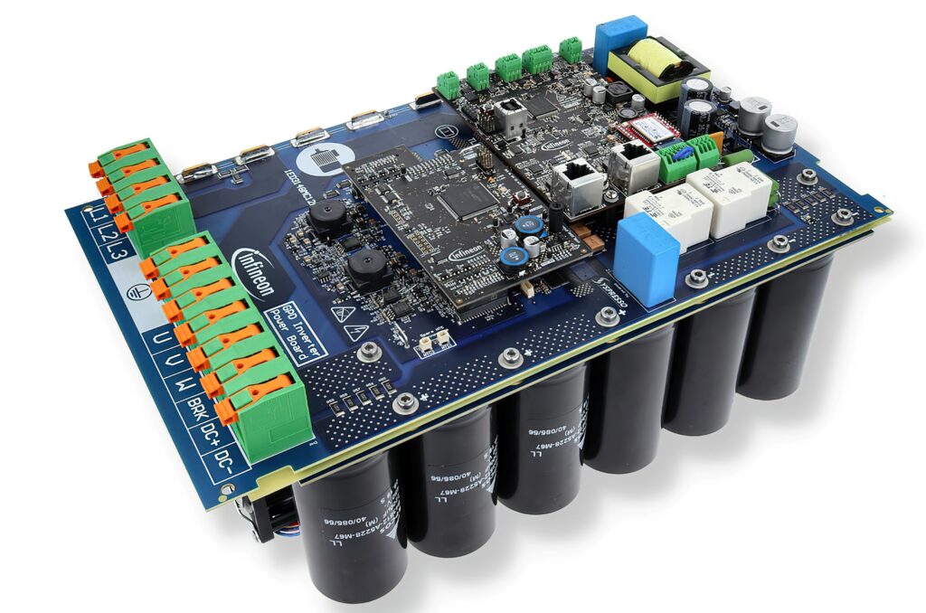
(Courtesy of Infineon Technologies)
Power Lifters
Nick Flaherty examines how new technologies are boosting the performance of inverters and onboard chargers
Switching is at the heart of the electrical systems for e-mobility platforms. The performance of the switching devices – the transistors – determines the power levels, the efficiency and even the size of the systems. Switching at higher frequencies reduces the size of the magnetics and allows more integration, lower weights and longer range
New types of transistors are opening up the use of switching topologies such as totem poles and Vienna rectifiers, which offer higher efficiencies than present switching topologies used with silicon MOSFETs and IGBTs.
However, there are distinctly different choices of devices, topologies and control schemes that can be used for switching in the inverter and onboard charger.
The 900 and 1200 V silicon IGBTs used in inverters to drive an EV’s motor typically switch at 10-20 kHz. MOSFET transistors built on silicon carbide (SiC) can switch at frequencies of 100-200 kHz, with efficiencies of about 97%. This higher efficiency means smaller, lighter heatsinks can be used, saving weight and cost.
IGBTs have better short-circuit withstand time, but higher switching losses. For SiC, the withstand time is shorter but there are lower losses that don’t increase with the breakdown voltage, giving designers more margin.
However, the SIC devices can be three times more expensive than IGBTs, and currently extend to 1200 V, which is sufficient for 800 and 900 V battery packs in e-mobility designs but can struggle as packs move to 100 V and above. IGBTs meanwhile can extend to 1700 V and even up to 3300 V for higher voltage switching systems in agricultural and construction platforms, where higher speed switching is not so important.
There are also hybrid devices, called cascodes, that combine an SiC transistor with a silicon IGBT or MOSFET in the same package to provide a balance of switching performance and cost.
The higher withstand voltage allows a single transistor to be used for each ‘leg’ of a switching architecture to handle a single phase, although lower voltage parts can be used in multi-stage designs. This become more complex though with multiple transistors for each stage and for each phase of the switching architecture.
“For 1200 V devices with an 800 V battery the IGBT is less competitive compared with SiC, but there are opportunities in charging applications,” says Luigi Di Turi, application manager for HV products at STMicroelectronics.
A newer generation of transistors using a layer of gallium nitride on a silicon substrate (GaN-on-Si) is being used in onboard chargers with new topologies such a totem pole or Vienna rectifier.
This is also leading to new algorithms to control the switching devices. Traditional switching control schemes such as pulse width modulation (PWM) are being enhanced with machine learning and new techniques to make the switching even more efficient.
Onboard chargers
With onboard chargers (OBCs), the silicon superjunction MOSFETs can be replaced by GaN or SiC devices, with the smaller size allowing the OBC to be combined with DC-DC converters.
“We start with the switching topologies rather than the technology,” says Di Turi. “The half-bridge arrangement is very versatile and can be implemented in an inverter with a leg of the bridge based on IGBT, SiC or a superjunction MOSFET. We also develop full-bridge and more complex switching topologies, implemented on the full primary side of an OBC with the rectifier. Switches with power levels of 2.2 to 3.3 kW could be IGBTs or SiC.”
The more complex topologies such as a totem pole design are switching below 70 kHz, typically at 30-40 kHz, where MOSFETs and IGBTs can be used. For example, STMicroelectronics has a 3.6 kW power factor correction reference design that uses a silicon carbide MOSFET switching at 72 kHz with an isolated FET driver controlled by a 32-bit microcontroller, with a peak efficiency of 97.5% and a total harmonic distortion of 3.7%.
“For the OBC the problem is there is both a single- and a three-phase input,” Di Turi says. “That means the topology has to move from single to three phase, and the Vienna rectifier is not suitable for this.
“There is still development with superjunction MOSFETs, and the devices are very efficient in DC-DC converter designs. Most of our customers prefer to use a variable frequency range of 120-200 kHz.
“With a GaN inverter the competition with SiC is complicated, as SiC is the acknowledged solution with a full-bridge topology with multiple devices per phase, while GaN requires a multi-level topology. The future of GaN is in the DC-DC or AC-DC portion of the charger in the kW range.
“With bidirectional charges the power must flow in both directions, so the hardware is two full bridges and there are a lot of PWM strategies for this. The choice of strategy depends on the power balance, whether it is the same power in both directions.
“For chargers using resonant switching at 3-5 kW that don’t need the same power rating in both directions, superfunction MOSFETs are still preferred. For an OBC rated to 22 kW where the power is almost the same in both directions and works at full load most of the time then SiC is preferred.”
Totem poles
All plug-in EVs require an OBC between the power grid and the HV battery pack, and this OBC needs a power factor correction (PFC) converter to connect directly to the grid to maximise the real power that flows.
Conventional PFC converters implement a passive diode bridge for rectification, which is now known as a passive PFC technique. This is a simple, reliable design with a slow control loop, but the passive components are heavy and generate significant power losses, resulting in bulky heat sinks and a lot of heat dissipation.
Owing to the various interoperability requirements, the industry uses many different PFC topologies. The vast majority of PFC stages in OBCs are operated in continuous current mode (CCM), which needs transistors that are robust against hard commutation on their body diode.
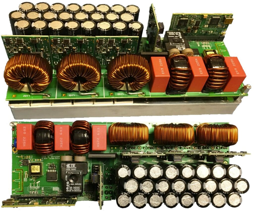
(Courtesy of Texas Instruments)
Superjunction devices, such as the CoolMOS CFD7A series from Infineon, can be used in CCM PFC stages with an SiC diode as the commutation partner. An alternative is to use either IGBT or CoolSiC wide-bandgap MOSFETs, as these technologies are inherently robust against hard commutation. In this case, two switches can be used in a half-bridge configuration, whereas the superjunction MOSFET works in combination with an SiC diode.
The input bridge consumes about 2% of the input power at the low end of a wide input voltage range. If the designer can suppress one of the series diodes they can save 1% of the input power, which allows the efficiency to rise from 94% to 95%, but this can limit the power capability of the OBC.
As a result, the trend is to eliminate the traditional diode bridge by using a SiC MOSFET switch.
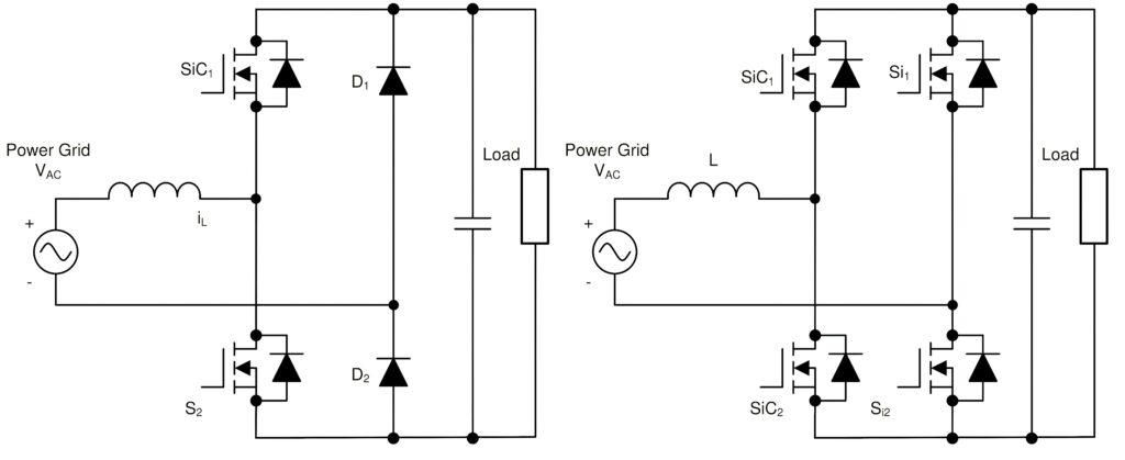
A totem-pole bridgeless PFC boost rectifier consists of a boost inductor, two high-frequency boost SiC switches (SiC1 and SiC2 in figure X above) and two components for conducting current at the line frequency. The line frequency components can be two slow diodes, as Fig. 1 shows. The left side shows two silicon MOSFETs (Si1 and Si2 ). The right side shows that the use of Si1 and Si2 further increases the efficiency.
The key issue in a totem pole PFC is the operation mode transition at the point the AC line crosses the zero-voltage line. When the AC input changes from the positive half line to the negative half line at the zero crossing, the duty ratio of the low-side high-frequency switch SiC2 changes from 100% to 0%, while the duty cycle of SiC1 changes from 0% to 100%.
Because of the slow reverse recovery of the high-side diode (or body diode of the MOSFET), the voltage at the cathode of diode D2 (in figure X above) cannot jump from ground to DC+ voltage instantly, and this causes a large current spike. Because of that, the designer cannot use a silicon MOSFET in a CCM totem-pole PFC.
This is where the SiC MOSFET and GaN transistors come in, as they have a low reverse recovery. The biggest advantage of the totem-pole PFC is the reduced power losses in the conduction path.
One 6.6 kW totem-pole bridgeless power factor correction design for an OBC uses SIC MOSFETs driven by a C2000 microcontroller (MCU) from Texas Instruments with SiC-isolated gate drivers. The design implements three-phase interleaving and operates in CCM to achieve a 98.6% efficiency at a 240 V input voltage and 6.6 kW full power.

The C2000 enables phase shedding and adaptive deadtime control to improve the power factor at light load. The gate driver board implements reinforced isolation and can withstand more than 100 V/ns common-mode transient immunity. The gate driver board also contains a two-level turn-off circuit, which protects the MOSFET from voltage overshoot during a short-circuit.
“If you are looking at just OBCs, the topology of the PFC is driven by the power level, and then you get all the other factors – faster charging, higher efficiency, smaller size then cost considerations,” says Jay Nagle, senior product marketing engineer for the automotive market segment at onsemi.
“We are seeing 3.3 kW OBCs with a single-phase boost PFC using one power switch and single diode, then interleaved multiphase boost to get to 6.6 and 7.2 kW.
“The three-phase totem pole is used for power levels of 11-22 kW, and this raises the fundamental question of whether to use SiC and GaN,” he says. “GaN does not have the same power density as SiC and has limited avalanche capacity, so it struggles to handle voltage stresses beyond the rated voltage so you have to be careful in fast switching configurations at high frequencies with lots of overshoot.
“Bidirectional OBCs need efficient use of the body diode, and SiC has zero reverse recovery so there are advantages there.”
That said, Navitas and Xaomi have shown a 6.6 kW OBC design using GaN with a 240-420 V output in a package measuring only 222 x 168 x 60 mm, and with a power density of 3 kW/litre – three times higher than silicon-based OBCs. Navitas says its OBC roadmap continues to more than 5 kW/litre.
(Courtesy of Texas Instruments)
VisIC, in Israel, has used a different type of GaN device in depletion mode to achieve a 100 kW inverter switching at 40 kHz. The depletion-mode GaN transistor is ‘normally on’ when the device is on with a gate-source voltage (Vgs) of 0 V and requires a negative Vgs to turn off.
D-mode transistors have been turned into normally off devices by using a proprietary normally off circuit and driving scheme. This D3GaN technology is used in a 100 kW inverter reference design that can be adapted to work on an 800 V or 900 V power bus. The inverter measures 26.9 x 21.4 x 3.5 cm and has a power density of 50 kW/litre. VisIC has also developed a 6.7 kW OBC providing a power density close to 3 kW/litre.
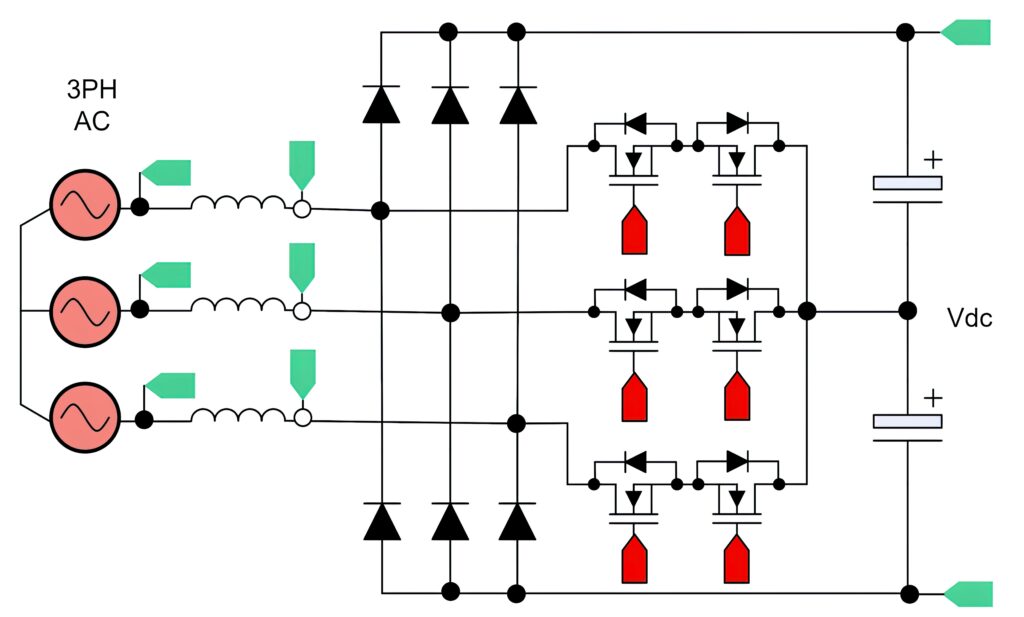
Vienna rectifiers
Although many topologies exist for active three-phase power factor conversion, a Vienna rectifier is popular owing to its operation in CCM and supports multi-level switching with less voltage stress on the power devices.
The Vienna rectifier is a unidirectional three-phase, three-switch, three-level PWM rectifier – essentially a three-phase diode bridge with an integrated boost converter – and traditionally uses a hysteresis-based controller. The unidirectional design means it is more suited to on-street or parking chargers, and the switching architecture can support higher power such as 350 kW fast-charging designs.
(Courtesy of Texas Instruments)
Modules
Having discrete transistors gives designers more flexibility in implementing whichever switching topology suits the design, but this is more complex in terms of assembly and cooling. Suppliers increasingly provide the transistors in modules on specialist substrates, which allows the inductance and parasitic capacitance of the connections to be minimised, helping to reduce the switching losses and boost the efficiency.
The modules started off as full-bridge and half-bridge implementations, with superjunction or SiC MOSFET transistors as the most flexible design option, but more are being developed to support a totem pole topology for the PFC stage in an OBC for example.
“Modules limit the choice of topologies, but with the module you have multiple die in a particular configuration in the package so you can save on system cost, so instead of using 36 discrete devices, it’s one package,” says Nagel. “The way the modules are pinned out allows us to connect the module to the DC busbar, and that gives the advantage of reducing the interconnect inductances.”
Switching controllers
New switching techniques are also being developed to boost the efficiency of inverters using IGBTs and SiC MOSFETs from low to high loads.
One of these, Optimised Pulse Pattern (OPP) modulation, is used to increase the efficiency of the inverter and the permanent magnet synchronous drive motor by reducing switching losses in the inverter and copper and iron losses in the electric motor.
This is achieved by dynamically switching the control of the modulation between speed/torque operating set points using several optimisation criteria but requires a high-performance controller. This can reduce losses by 2 to 5 percentage points in the motor and inverter.
OPP is based on field-oriented control of the current/torque regulation and adaptive PWM control of the modulation. Depending on the motor’s operating conditions, the controller can switch between different types of modulation techniques to provide the optimal modulation for the targeted set point.
OPP uses a set of switching (pulse) patterns that are pre-computed offline to reduce switching losses in the iron and copper of the motor using precisely pre-calculated switching angle positions. The duration and position of the pulses are determined from the voltage modulation ratio and e-motor speed. Combined with voltage phase compensation, the optimal operating range of the electric motor can be extended, reducing losses, torque ripple and total harmonic distortions, thus improving the overall system’s efficiency.
Traditional space vector PWM (SVPWM) is based on fixed switching frequencies, where only the PWM duty cycle varies, while the number of switches per time period is fixed. Improving the quality and efficiency of an SVPWM-controlled inverter means finding an optimal switching frequency, which is a compromise between losses in the inverter and the quality of the sinusoidal phase currents. Increasing the frequency of the SVPWM increases the quality of the output currents, but at the expense of a dramatic increase in the inverter’s switching losses.
Instead of modulating a duty cycle at a fixed time intervals (frequency), OPP is based on periodic switching patterns that are generated as a function of the position of the electric motor.
However, OPP execution demands a huge real-time processing capability. As an example, for a six pole-pairs electric motor rotating at 20,000 rpm, controlled with modulation over 32,768 cycles, a software implementation of OPP would require 65,536,000 interrupts/second. A software-based implementation in a processor cannot properly support such a modulation. Currently, the field-programmable control unit (FPCU) from OLEA is the only automotive-qualified system-on-chip powerful enough to run the algorithm, while also ensuring the ISO 26262 safety ASIL D level.
The unit been tested on a two-level, 400 V inverter from BorgWarner/Cascadia Motion (the PM100DX) with a control board including an OLEA T222 FPCU from Silicon Mobility and a Semikron IGBT module. The motor is an HVH250-090SOM product from BorgWarner. The tests show an increase in efficiency of the IGBT-based switching system from 82 to 87% at low load and from 91 to 93% at higher loads.
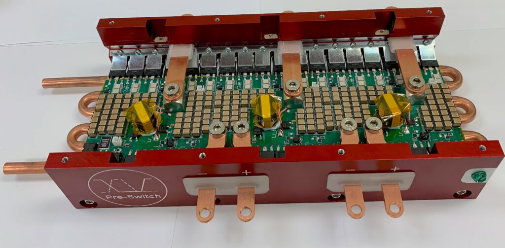
Pre-switching
Another approach is pre-switching, where the timing of the switching is varied according to changes in the inductance and capacitance of the inverter. These vary with the load, so the timing of the switching is constantly changing.
“If you look at a Tesla, the drivetrain is the biggest loss in the system until 55 mph, then wind resistance becomes the biggest loss,” says Bruce Renouard, CEO at Pre-Switch. “This means you have a different efficiency at 5-6% load and at 80% load, but the efficiency of pre-switching is flat across the load.”
This pre-switching is achieved by a combination of a new switching topology and a controller called CleanWave, which uses machine learning to identify the patterns in the voltage and current across the combination of the inverter and the motor, and across the whole load range. The controller pre-distorts the sine wave that controls the switching of the transistors so that a perfect sine wave is recreated in the motor.
“We add two IGBT switches to a half-bridge to handle the current for a pulse rating with zero switching losses so that they can switch faster,” Renouard says. “That means they don’t need to be big, which means you can reduce the size of the working switches, from four or six units in parallel to each other. The other benefit is that you shrink the DC link capacitor dramatically.”
“We gave one design a 0.5% gain in peak efficiency but at the 5% load it’s a big difference, it gives 5-12% more range.”
(Courtesy of onsemi)
“We are giving people a full inverter with motor control that we will license, but we have also developed a 200 kW inverter that is 32 mm tall, 150mm (6 in) wide and 200mm (8 in) long including all the cooling and DC link capacitor,” he says. This smaller size comes mainly from reducing the size of the DC link capacitors, as they have to handle less current.

“The CleanWave2 design uses the cheapest IGBTs and cheapest discrete SiC cascode devices,” he adds. These cascode devices, from UnitedSiC, combine a low-voltage silicon MOSFET and high-voltage SiC JFET (junction FET) in the same package. Their advantage comes from the fact that they can be controlled using ordinary MOSFET gate-drive signals generated by an ordinary MOSFET gate driver.
“You can’t usually use these in inverters, as they are not gate-controlled, so you can only use them in a soft switching topology. But with our topology there is no damping as switching occurs with zero voltage and zero current. This design is for frequencies from 50 to 150 kHz with no external DC link capacitors.”
“By doing the whole motor control we were able to improve the efficiency of the whole system,” he says. “Working with other people’s inverter designs, we had to react to the PWM input and map the performance over a period of time to learn the system. Now we know what the system needs and how it works. For example, this means at peak load we can slow the switching down to 10 kHz, where the edge is transitioning the fastest across the zero voltage, and that’s how we reduce the losses.”
While the initial interest is in improving the efficiency of low cost IGBT-based inverters, the technique can be applied to SiC and GaN-based topologies to reduce the size of the inverters even further.
“We think high switching frequency will be a key differentiating technology; we can work with GaN and we have done SiC at 1 MHz,” Renouard says. “It’s all about the dv/dt in the wires of the motors – we make the edges very smooth, we slow down the edges and speed up the transitions to reduce the current in the system so the conduction losses are low, but the switching losses stay the same. With pre-switch, there are no switching losses so there is no fall-off as the load increases.”
“We can work with other switching architectures – we are not tied to PWM, although we have a customer looking at a DC-DC converter project for its smallest electric truck,” he said.
(Courtesy of Pre-Switch)
Safety
The UnitedSiC cascode devices have moved from OBC and DC-DC designs to inverters. “These are used in traction inverters with sophisticated control schemes,” says Dr Chris Dries, chief executive and founder of UnitedSiC, which is now part of Qorvo.
“The low on-resistance of the JFET cascodes allows us to really exploit areas of functional safety to provide circuit protection. For example, rather than having a mechanical switch creating the connection between the high-voltage switching and the electronics, you can replace this with a solid state switch using the cascode.
“We have a number of designs in the US and Europe all using our discrete devices in 400 V inverter designs, with the 750 V devices with 5.9mΩ on-resistance and in 800 V inverter designs with 1200 V class devices.” This is increasingly being adopted in industrial EVs such as forklifts with a 400 or 500 V inverter using a phase shift full-bridge topology.
Conclusion
Advances in powertrain design come from a combination of wide-bandgap materials such as GaN and SiC, new device combinations such as cascodes, new topologies and new controller architectures. All of these can be used in different ways to reduce the parasitic losses that lower the efficiency of the inverter and the bidirectional onboard charger.
The controllers can boost the performance of the switching of silicon IGBT transistors to boost the performance of existing topologies, and can be used with new topologies to provide higher efficiency across the whole load profile of a powertrain.
New transistor devices using SiC can handle higher power with lower losses and higher frequencies than IGBTs and superjunction MOSFETs, while depletion-mode GaN transistors can switch in the MHz range. These higher switching speeds can reduce the size of the magnetics used in topologies such as totem poles for OBCs and Vienna rectifiers for on street chargers. That helps to reduce the size and weight of the on-board chargers, reducing the weight of a vehicle and improving the efficiency of the fast chargers.
ONLINE PARTNERS
