


Wide bandgap materials

(Image: Toyota)
Powering beyond silicon
The shift to wide bandgap materials isn’t just an incremental upgrade, it is the fundamental enabler for the next generation of high-performance, long-range EVs, reports Nick Flaherty
Wide bandgap (WBG) materials – primarily silicon carbide (SiC) and gallium nitride (GaN), but also gallium oxide (Ga2O3 or GaO) – are defined by their electronic bandgap energy, which is significantly higher than that of traditional silicon at 1.1 eV. Specifically, SiC and GaN possess bandgaps of approximately 3.2 and 3.4 eV, respectively, with GaO at 4.5–4.9 eV. This physical property allows these semiconductors to withstand much higher breakdown electric fields and operate at significantly higher temperatures than silicon-based components.
Their primary advantage in EV powertrains is the reduction of switching and conduction losses. The on-resistance (RDS(on)) of a WBG material is significantly lower than that of silicon, reducing the conduction losses, while WBG materials can also switch at much higher frequencies (in the MHz range for GaN) to minimise the energy lost as heat during each cycle.
This combination directly translates to extended range because more energy from the battery reaches the motor rather than being dissipated as heat. This also simplifies the cooling system with smaller, lighter heat sinks for more compact inverters.
By operating at higher frequencies, WBG-based inverters can also use much smaller passive components, such as inductors and capacitors. A WBG-based inverter, using either SiC or GaN, can be up to 50% smaller than its silicon counterpart.
(Image: Microchip)
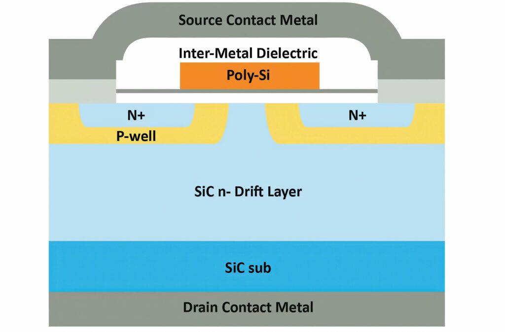
Silicon carbide
SiC switches use a MOSFET field effect transistor structure. The devices started out as lateral, planar devices, but recent innovations have created trench versions and hybrids that combine both trench and planar features.
The more mature planar technology features a horizontal channel on top of the SiC wafer, offering higher, more robust reliability, better avalanche energy and simpler manufacturing, making them common in high-voltage applications.
Trench SiC MOSFETs use a vertical channel (a groove) to reduce the on-resistance and cell size, although they face challenges with gate oxide field concentration at the trench bottom.
Trench-Assisted Planar is a hybrid approach that uses a planar gate structure to balance the high-efficiency benefits of trench technology with the reliability of planar fabrication.
There are two key features to the SiC MOSFET: the body diode and the short-circuit robustness.
Every SiC MOSFET has an intrinsic body diode formed by the junction between the P-well and the N-drift layer. In EV inverters, this diode is critical because it handles ‘freewheeling’ currents when the transistor is turned off.
SiC body diodes have extremely low reverse recovery charge. In silicon MOSFETs, when the diode switches off, a burst of stored charge flows backward, causing massive energy loss. In SiC, this recovery is nearly instantaneous, drastically reducing switching losses.
However, the forward voltage drop of a SiC body diode is high compared with that of silicon. To prevent efficiency loss, engineers often use synchronous rectification, turning the MOSFET channel back on to bypass the diode.
(Image: Rohm)

(Image: CISSOID)
Short-circuit robustness
The ability of the device to survive a massive current spike until the protection electronics can shut it down, is characterised by its short-circuit ruggedness.
Because SiC MOSFETs are much smaller than silicon IGBTs, they have less thermal mass. During a short-circuit, the current density is so high that the temperature at the gate oxide can skyrocket in microseconds.
Traditional silicon MOSFETs can often survive a short-circuit for 10 μs. However, owing to the vertical structure and high current density of SiC, the short-circuit withstand time is often much lower – typically 2–5 μs. This requires fast desaturation detection in the gate driver, and the driver must sense the fault and turn off the gate before the device melts.
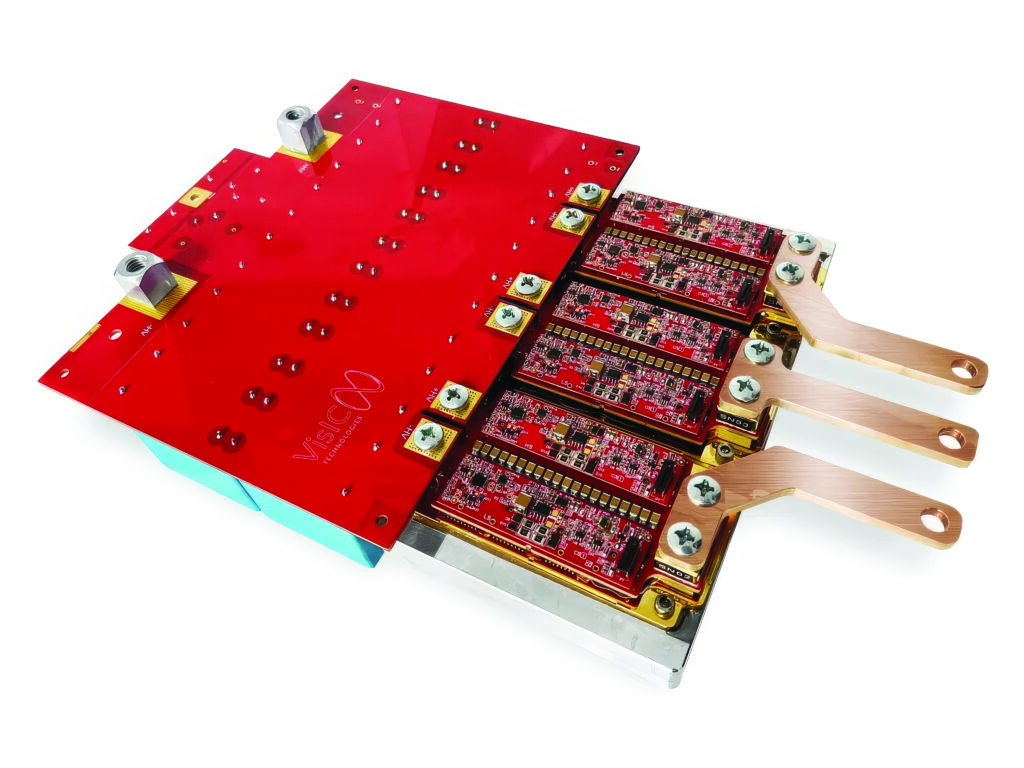
(Image: VisIC Technologies)
SiC switching
The speed at which a transistor switches is primarily limited by how quickly you can move charge in and out of its internal structures. At around 200 kHz, a SiC MOSFET switches faster than a silicon IGBT at 5–10 kHz. This comes from three fundamental physical advantages.
The most significant factor is that a SiC device has a critical electric field that is about 10 times higher than that of silicon, which requires a thick, lightly doped drift region to handle high voltages of up to 1200 V for 800 V EV designs.
Because SiC can withstand higher voltage per micrometre, the device can be made 10 times thinner with higher doping levels. A thinner device means that electrons have a much shorter distance to travel and the internal capacitances are significantly reduced.
Switching speed is essentially governed by the resistance-capacitance) time constant. To turn a MOSFET on or off, the gate driver must charge or discharge internal parasitic capacitance between the gate, source and drain.
SiC devices are physically much smaller than silicon IGBTs for the same power rating, meaning that the capacitances are reduced. With less charge to move, the device can transition between the on and off states in nanoseconds rather than microseconds.
IGBTs are bipolar and use both electrons and ‘holes’ to carry current. When the IGBT switches off, the holes don’t disappear instantly and must recombine, creating a tail current that slows down the switch and generates heat.
Conversely, SiC MOSFETs are unipolar and only use electrons, so there is no stored charge to wait for, meaning that the current can be cut off almost instantly without a tail.
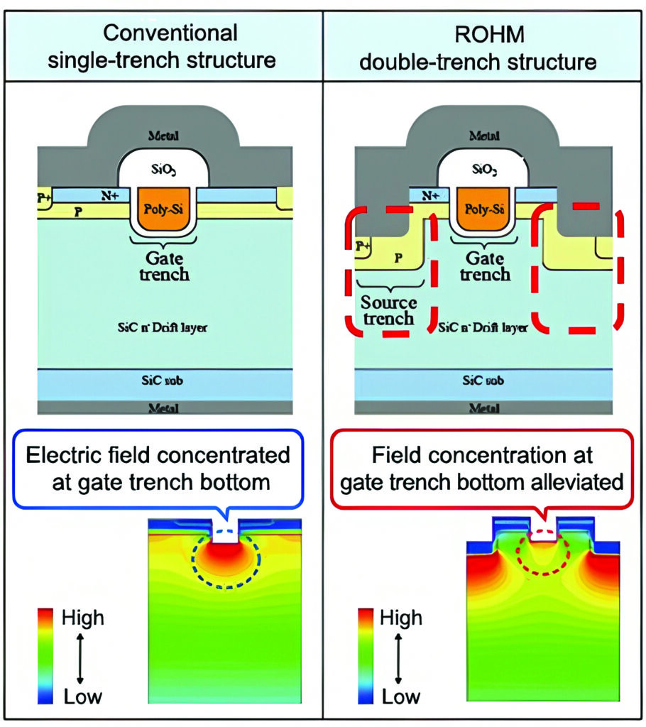
Trench SiC
Trench SiC MOSFETs feature a specialised, high-integration structure designed to reduce power loss by approximately 50% compared with that of conventional planar devices.
Trench structures are widely used in silicon MOSFETs, and the use of trench structures in SiC MOSFETs has attracted attention because of the effectiveness in lowering the on-resistance.
However, in typical single-trench structures, the electric field is concentrated at the bottom of the gate trench, and so long-term reliability has been an issue. In the double-trench structure, a trench structure is provided in the source area as well, meaning that the electric field concentration at the bottom of the gate trench is alleviated and long-term reliability is secured, making possible mass production.
SiC MOSFETs that adopt this double-trench structure have on-resistances reduced by about 50%, and input capacitance reduced by about 35%, compared with second-generation planar-type SiC MOSFETs already in mass production.
Another design uses a vertical, trench-gate structure with key features including a bottom P-type protective layer (BPW) to manage electric fields, sidewall P-type pillars (SP) for grounding, and an N-type JFET doping layer to maintain low on-resistance.
The BPW is a P-type region at the bottom of the trench that protects the gate oxide layer from high electric fields, improving reliability. The SP is a P-type pillar along the trench sidewalls that connects to the BPW, ensuring stable, high-voltage operation.
An N-type layer prevents the current path from narrowing, helping to achieve low on-resistance while a vertical structure enhances current density and improves on-resistance. All of these structures can be built with tilted ion implantation, which is a simplified manufacturing process.
(Image: Cambridge GaN Devices)
Manufacturing
SiC devices, despite being in mass production, haven’t yet reached their full potential in terms of performance and reliability.
A two-step, high-temperature hydrogen annealing process, performed before and after gate oxide deposition, could drastically improve both performance and reliability without introducing impurities that can be a problem for performance. A new process effectively removes defects at the oxide–SiC interface, resulting in a lower interface state density and higher channel mobility. This improves immunity against both positive and negative bias stress, expanding the operational voltage range.
By enhancing the reliability and performance of SiC MOSFET devices, this technique paves the way for their wider adoption and contributes towards a more energy-efficient future.
End-to-end design
Designing the gate driver to match the specific device characteristics has enabled higher levels of efficiency and new architectures that simplify the generation of the signals that drive the motor. This further helps increase the efficiency and reduce the heat losses.
For example, a 100 kW inverter with 94% efficient silicon IGBT devices loses 6 kW in heat. Reducing that to 1 kW with a 99% efficient SiC design dramatically reduces the thermal management requirements, saving cost, space and weight.
This is possible through optimisation of the gate driver with the SiC transistors in a module and a new generation of software. These are currently aimed at heavy-duty applications that tend to be lower volume but have higher demand on the specification.
The additional innovation is in the software rather than the hardware. This uses dead time compensation to provide a smoother sinusoid signal that is tuned to the module to compensate for dead time.
This approach reduces the noise floor to 5 dB from 30 dB and means there is a lot less noise going into the motor. As a result, the size of the motor can be reduced, saving weight. This also allows for a smaller DC-link capacitor to be used.
This moves away from fixed switching to a pre-generated pattern of optimised pulse patterns that are pulled out of a lookup table. This pattern can optimise for the motor and the behaviour – optimising for the total harmonic distortion as well as the balance of the inverter and the motor – reducing the ripple, noise and vibration for a specific inverter–motor combination.
This is implemented with an approach that is halfway between offline measurements and real-time calculation. If the sense of the current is known, the overhead can be reduced such that one quadrant of a cycle can fit into a microcontroller and be duplicated and inverted where needed. This also leaves enough room for customisation for the customer.
Additionally, this allows the spikes of the switching to be placed anywhere in the cycle, away from the traditional 12 or 16 kHz switching waveform that can be used to tune how the motor sounds as well as enabling efficiency of 98–99%. It also allows for a lower bus voltage.
(Image: University of Nagoya)
GaN
GaN can provide higher efficiency with a smaller footprint power conversion in EVs, but adoption of the technology faces some significant challenges around using the devices in applications.
GaN, a WBG material like SiC, offers higher electron mobility, enabling switching up to 10 times faster than SiC and nearly 100 times faster than IGBTs. This reduces the size of the magnetics, inductors and capacitors. GaN FETs lack body diodes, avoiding reverse recovery losses and improving efficiency in hard-switching set-ups, while also simplifying parallel operation challenges such as current sharing and switching stress.
Compared with IGBT or SiC devices with similar power ratings, GaN devices are physically smaller, allowing tighter PCB layouts. This minimises loop and stray inductance, enabling closer placement of devices and reducing issues like oscillation and ringing during paralleling.
There are two types of GaN structure and both can be used for EVs.
Depletion-mode (d-mode) GaN transistors are ‘normally-on’ devices. Without any applied gate voltage, the conducting channel is already open, allowing current to flow. To turn the device off, a negative voltage relative to the source needs to be applied.
This normally-on behaviour is a safety risk in power applications; if the controller loses power, the switch stays closed, potentially causing a short-circuit. This means most d-mode GaN is used in a cascode configuration, pairing it with a low-voltage silicon MOSFET to make it behave like a ‘normally-off’ switch.
A d-mode GaN inverter reached a benchmark efficiency level of 99.67% at 10 kHz, climbing to over 99.8% efficiency at 5 kHz, outperforming comparable SiC inverters by up to 0.5% and cutting energy losses by more than 60%.
A new generation of d-mode GaN devices is being developed with a breakdown voltage of 1350 V to address 800 and 1000 V powertrains directly rather than having to use a multilevel architecture with 650 or 750 V devices.
Enhanced-mode (e-mode) GaN transistors are normally-off, mirroring the behaviour of traditional silicon MOSFETs. The channel is closed at a gate voltage of 0 V and only begins to conduct once a positive threshold voltage is applied.
Because they don’t require a cascode device, e-mode devices are simpler, smaller and offer lower parasitic inductance. However, they have a very narrow gate voltage range, often limited to 6 or 7 V, making them more sensitive to voltage spikes than the d-mode version.
E-bikes
A 3-phase BLDC motor drive inverter using an e-mode GaN FET for e-bikes operates with a wide input DC voltage ranging from 14 to 65 V and has two configurations: a standard unit and a high-current version.
The standard reference design uses a single FET for each switch position and can deliver up to 30 ARMS maximum output current. The high-current configuration version of the reference design uses two paralleled FETs per switch position with the ability to deliver up to 60 Apk (42 ARMS) maximum output current.
Both versions contain all the necessary critical function circuits to support a complete motor drive inverter including gate drivers, regulated auxiliary power rails for housekeeping supplies, voltage and temperature sense, accurate current sense, and protection functions in a board that measures just 130 mm x 100 mm including the connector.
A GaN-base motor drive has lower distortion for lower acoustic noise, lower current ripple for reduced magnetic loss and lower torque ripple for improved precision. The small size allows integration into the motor housing resulting in the lowest EMI, highest density and lowest weight.
The development of an interface to simplify the use of GaN transistors allows for higher-frequency operation and allows for smaller magnetics to reduce the size and weight of the power converters. This also opens up opportunities in the powertrain of EVs.
A series of techniques allows GaN devices to be used in parallel. This can reduce the size of the power system and the inverter while improving the efficiency and reducing the cost of an inverter design compared with SiC.
GaN interface
Adding an interface to a 650 V GaN transistor with low RDS(on) makes it easier to use in automotive power systems. This enables standard gate driver chips that provide voltages of 20–22 V to be used, streamlining sourcing and reliability of gate drivers while allowing for greater efficiency and compact designs.
This integration enables a low-profile, low-inductance package, reducing losses and improving power converter efficiency.
The interface incorporates a built-in Miller clamp using a high-electron-mobility transistor (HEMT) device rather than an e-mode FET, establishing a
2.9 V threshold voltage and avoiding the requirement for negative gate voltages to maintain the device in the off state. This clamp increases the safe operating area and improves gate reliability by accommodating higher dV/dt rates. Additionally, designers may optimise the switching speed by selecting an appropriate turn-on driving resistor, achieving an effective balance between EMI mitigation and switching losses without the need for supplementary negative voltage rails.
The key to the improved transfer characteristic in the interface is an auxiliary HEMT. This allows the external gate to exceed the 6 V typically specified by a discrete e-mode GaN. The current source provides a constant current to the voltage limiter, which clamps the gate of the auxiliary HEMT approximately to a threshold above the desired gate voltage of the main power HEMT.
The internal gate of the HEMT only begins to increase once the external gate has exceeded approximately
1.5 V. It is this additional threshold that allows the device to have a higher threshold voltage than a conventional discrete e-mode GaN at 2.9 V. Once the gate voltage reaches 4.7 V, it begins to become clamped through a combination of a current source and voltage limiter setting the gate voltage of the auxiliary HEMT. This limits the current consumption in this clamping condition and keeps the gate driving losses at an acceptable level.
A major advantage of GaN HEMT devices is their excellent switching performance, which results from a very low gate charge and the absence of a body diode – leading to virtually no turn-off losses. The Miller clamp switches the device off at zero volts; therefore, the interface avoids the losses that can affect other GaN components.
Another feature of GaN is the positive temperature coefficient. This means that as the temperature of the device increases, the resistance also rises.
The smart interface opens up further opportunities for parallel operation of multiple GaN devices in the powertrain. There has been a challenge using more than two GaN in parallel in power supply designs, arising largely from the difficulty in balancing the gate drive voltages and using the negative voltage to switch the device off.
When several devices are connected in parallel, they must be switched synchronously. Therefore, using a single gate driver will minimise any synchronisation issues that may result from using individual gate drivers for each device in parallel. This requires a single gate driver to support the driving of several devices.
The 2.9 V threshold of the Miller clamp also allows the GaN switch to provide more headroom to avoid spurious switching signals that can interfere with the quality of the sinusoidal output.
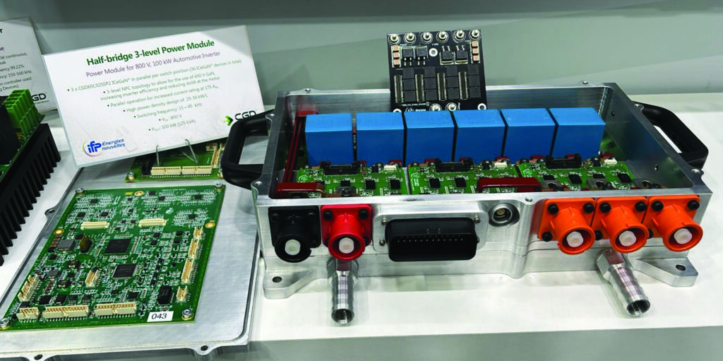
Prototype implementation
A demonstration system was developed with GaN devices with this interface in a multilevel, 800 VDC inverter. The demo uses 36 650 V devices in parallel in three levels and achieves power density of 30 kW/L, which is greater than can be achieved by more expensive SiC devices.
This multilevel GaN inverter can power electric motors to over 100 kW peak, 75 kW continuous power with a peak current of 125 ARMS for 10 s (180 Apk) and a continuous current of 85 ARMS (120 Apk).
Using an array of GaN devices in parallel provides higher efficiency of 99.1%, up from 95% for IGBT silicon devices. This translates into increased battery range and reduced charging cycles. It also leads to reduction in battery cost for the initial range. The GaN transistors can operate at much higher frequencies than silicon transistors, which helps to reduce the losses in the motor, particularly in the case of machines with low inductances.
The 3-level topology minimises EMI with lower total harmonic distortion and enhances the reliability of the system. This also allows insulated metallised substrate boards with an aluminium core to be used, supporting higher thermal dissipation, ensuring optimal operating temperatures and again improving the reliability of the inverter. The design is modular and so can be scaled to meet lower power requirements, again with high levels of efficiency.
Combo design
Using different technologies in parallel can be a way to combine cost and performance.
The combo approach uses the fact that GaN and IGBT devices can be operated in a parallel architecture having similar drive voltage ranges (e.g., 0–20 V) and excellent gate robustness.
The combo design also benefits from the high saturation currents and avalanche clamping capability of IGBTs and the very efficient switching of GaN. At higher temperatures, the bipolar component of the IGBT will start to conduct at lower on-state voltages, supplementing the loss of current in the GaN. Conversely, at lower temperatures, GaN will take more current. Sensing and protection functions are intelligently managed to optimally drive the combo GaN and enhance the safe operating area of both the GaN and the IGBT devices.
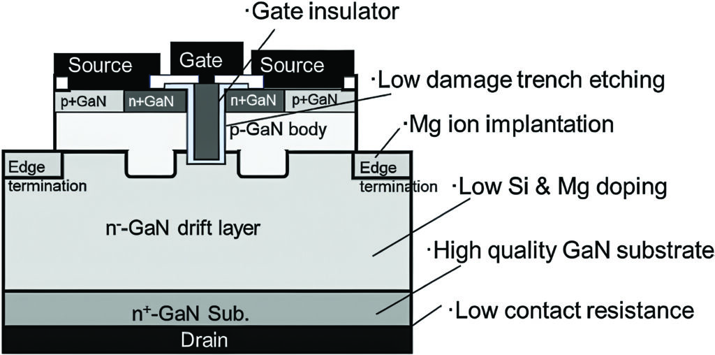
Vertical GaN
Even today, one of the major obstacles preventing practical application of vertical GaN structures is the immaturity of key manufacturing processes. For vertical GaN devices, reliable and reproducible process technologies, such as low-damage dry etching, selective doping, high-quality gate dielectric formation and stable ohmic contact formation are essential for achieving both high performance and manufacturability. This is enabling MOSFET structures rather than the current planar HEMT structures.
GaN MOSFETs potentially have higher power-handling capabilities, increased current density and better voltage blocking owing to the 3D vertical current conduction. While GaN HEMTs excel in high-speed, low-to-mid-power applications, GaN MOSFETs provide better robustness for high-voltage, high-power systems by eliminating surface trapping effects.
The trench serving as the gate region in trench MOSFETs is formed by dry etching. Two major requirements must be considered in trench formation. First, the trench geometry must be optimised: the sidewalls, which form the current path, should be flat and the bottom corners – where electric field crowding tends to occur – should preferably be rounded. Second, no etching-induced damage should remain on the sidewall surfaces because such damage degrades the channel mobility and consequently increases the device’s on-resistance.
An integrated process for trench MOSFETs with a vertical drift layer has been developed to evaluate the basic characteristics of the vertical MOSFET, including on-resistance, breakdown voltage and channel mobility.
This requires new types of p-type ion implantation and activation processes, integrated with epitaxial processes for the substrate to provide both high breakdown performance and reduce the on-resistance.
Gallium oxide
GaO is a semiconductor material that could make electronic devices much more energy-efficient than current silicon-based technology. Electronic diodes require both p-type and n-type layers. Scientists could reliably produce n-type GaO layers but struggled to create stable p-type layers because the GaO crystal structure naturally resists the atoms needed for these layers. This limitation resulted in GaO semiconductors with poor performance and reliability issues.
A new method enables the use of GaO for pn diodes that can carry twice as much electrical current as previous GaO diodes, and GaO pn diodes can handle twice the current capacity of previous GaO devices and waste less energy than silicon-based diodes. This makes them suitable for demanding applications and translates to reduced cooling requirements, better energy efficiency in high-power systems and lower operating costs.
The problem was that the crystal structure of GaO easily accepts the atoms needed to create n-type layers but rejects the atoms required for p-type layers. Previous methods to force them in either failed or required temperatures that destroyed the material. Without both types working together, GaO remained limited for practical applications.
To address this, nickel atoms are injected into the GaO layer by shooting individual atoms at high speed into the surface of the material. The material is heated twice, first at 300 C with activated oxygen radicals (oxygen atoms that have been given extra energy using a proprietary plasma treatment) and then at 950 C in oxygen gas. This converts the embedded nickel into nickel oxide that is properly integrated with the GaO crystal structure.
This method uses standard industrial equipment and processes, meaning that it can be scaled for mass production.
Conclusion
WBG materials are pushing into the powertrain of EVs, with lower on-resistance and higher-frequency operation compared with silicon IGBTs.
SiC is well established in the move from planar to trench structures, reducing the size, cost and on-resistance of the devices for inverters, while GaN MOSFETs are just starting that journey to vertical devices. Now, GaO oxide, with its even higher bandgap, is emerging as a potential technology that could outperform both in the long-term future.
Acknowledgements
With thanks to Mike Sandyck at CISSOID, and Professors Masaru Hori & Tetsu Kachi at Nagoya University for their help with this article.
Some suppliers of wide bandgap materials
BorgWarner
Bosch Semiconductors
Cambridge GaN Devices
Cascadia Motion
CISSOID
Eaton
Fuji Electric
hofer powertrain
Infineon Technologies
Microchip Technology
Mitsubishi Electric
Navitas
onsemi
Renesas Electric/Transphorm
Rohm
Schaeffler
SemiQ
StarPower Europe
STMicroelectronics
Texas Instruments
VisIC Technologies
Wolfspeed
ZF
www.borgwarner.com
www.bosch-semiconductors.com
www.camgandevices.com
www.cascadiamotion.com
www.cissoid.com
www.eaton.com
www.fujielectric.com
www.hoferpowertrain.com
www.infineon.com
www.microchip.com
www.mitsubishielectric.com
www.navitas.com
www.onsemi.com
www.renesas.com
www.rohm.com
www.schaeffler.com
www.semiq.com
www.starpowereurope.com
www.st.com
www.ti.com
www.visic-tech.com
www.wolfspeed.com
www.zf.com
Click here to read the latest issue of E-Mobility Engineering.
ONLINE PARTNERS
