


Power Semiconductors

(Image courtesy of EPC)
Cascade of power
Nick Flaherty discovers how the world of power semiconductor devices is shifting away from silicon
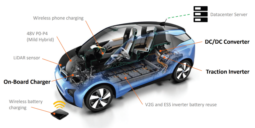
Power semiconductors are used across many areas of e-mobility, with different technologies suitable for each part of a vehicle, depending on the voltage and current requirements, while emerging tech is allowing smaller systems to be implemented.
As a result, the choice of power semiconductor now depends on the voltage, type of vehicle – whether e-bike, three-wheeler, truck or high-performance – and offroad equipment with higher current requirements. Similarly, the choice of power semi-conductor varies, depending on its usage in the vehicle platform, from the inverter to the DC-DC converter, the AC-DC charger or other motor-control applications.
New materials have emerged over the last decade alongside silicon that shave a wider electron bandgap, hence a wide bandgap (WBG), giving more flexibility in design and higher performance.
For example, the traction inverter is a stalwart area for silicon insulated-gate bipolar transistors (IGBT) that run up to 1200 V, and even 1700 V, but field-effect transistors (FETs) built on metal-oxide semiconductors (MOSFETs) with wide-bandgap silicon carbide (SiC) at 1200 V are becoming increasingly popular.
Another WBG material, gallium nitride (GaN), is being used as the level of voltage the devices can take – the ‘withstand voltage’ – increases. Rather than the bipolar transistor structure of the MOSFET, this uses a different structure with a high-energy mobility transistor (HEMT) switching a two-dimensional electron gas.
Meanwhile, in the AC-DC onboard charger and DC-DC converters, silicon MOSFETs are a mainstream device, but GaN is starting to dominate. It allows much higher switching frequencies for the power conversion, which means smaller, magnetic components are needed, saving space and weight. This becomes significant for light electric vehicle (LEVs) with two or three wheels.
All of these are built on wafers of silicon or silicon carbide but are manufactured with significantly different techniques to the silicon chips found in mobile phones or laptops.
(Image courtesy of STMicroelectronics)
Key considerations
As well as the withstand voltage, the ‘on resistance’ is a key parameter for a power semiconductor and it is measured in milliohms (mΩ). This is the resistance between the drain and the source in any transistor when it is switched on, and it is referred to as RDS(on). The lower this value, the lower the losses and the more efficient the transistor. However, the way to reduce resistance is to increase the size of the transistor as the current requirement increases, which also raises the cost.
As a result, device makers have moved from planar transistors that are spread out horizontally to a trench structure, which is built vertically. While this is more complex to make, the trench structure allows many more devices to be built on a silicon wafer, reducing the cost of each individual device.
IGBTs have moved from a planar structure to trench, driving down the cost, although large planar devices that withstand voltages up to 3300 V are still used for high-power traction applications, particularly for electric trains. Work is continuing to move silicon-carbide MOSFETs to trench structures as the wafers are an expensive material that is almost as hard, and expensive, as diamond.
While there is little drive to do the same for GaN, which uses a GaN layer on top of a silicon wafer, there are some projects working to do just that. The real promise for GaN is the ease of integrating the other control logic needed into one chip, further simplifying the design of the power system and reducing the cost.
However, designers want to use these newer power-transistor devices in the same way as MOSFETs and IGBTs, with the same chips that drive the gates of the transistors – the gate drivers.
There are also devices that add a SiC or GaN diode to a MOSFET in a cascode configuration. This is a mid-range solution with less performance than a pure SiC MOSFET or GaN high-electron mobility transistor (HEMT), but it boosts performance, and in many cases it simplifies the design by being a drop-in replacement for a silicon MOSFET device.
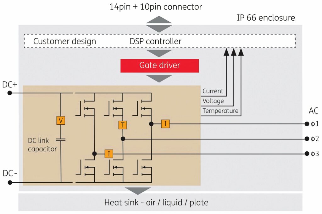
(Image courtesy of Semikron)
Packaging
The choice of packaging has a big role to play in the losses experienced with power semiconductors. For inverters, mounting the bare die in a high-end module on a ceramic substrate to carry away heat is a suitable approach, while plastic modules are popular for mainstream applications with ready-built, half-bridge topologies for power conversion.
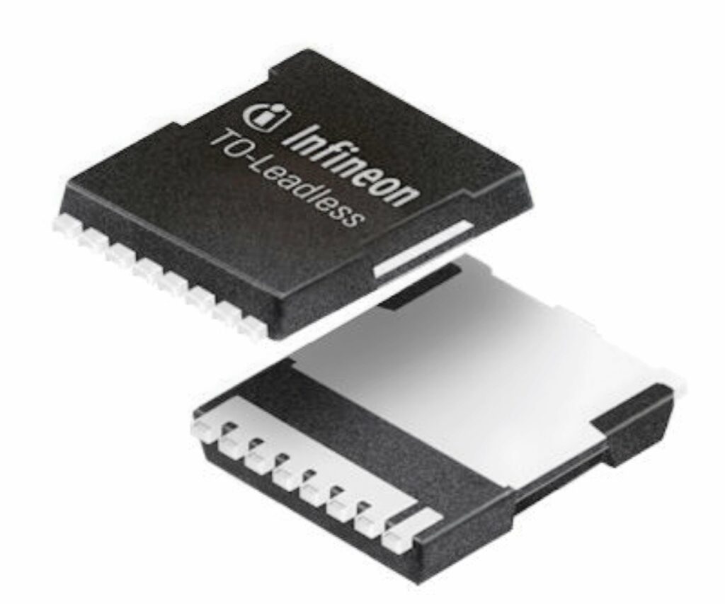
Discrete packages can be used for designers who want to build their own systems. While so-called Kelvin packages add an extra fourth leg to reduce overall resistance, there are transistor outline leadless (TOLL) packages that also reduce RDS(on).
For example, the 100 V automotive-qualified OptiMOS silicon MOSFET devices from Infineon Technologies support currents up to 300 A with RDS(on) down to 0.77 mΩ. This makes it possible to reduce the number of parallel MOSFETs in all high-current applications and boosts the power density of a design.
Compared with the previous seven-pin Double Decawatt Package (D2PAK), the TOLL devices have a 30% smaller footprint on a board and half the height, saving space. The lower package parasitic inductances also result in improved EMI behaviour. The 50% bigger solder contact area on the TOLL package also avoids electro-migration at high current levels, improving reliability.
Power semiconductor tech
(Image courtesy of Infineon Technologies)
The basic technologies for power are the bipolar junction transistor (BJT), MOSFET and IGBT. All have three main connections to the outside: a collector, emitter and base in the BJT; a gate, source and drain in the MOSFET; and a collector, gate and emitter in the IGBT.
The biggest difference at a fundamental level is how these semiconductor devices are driven, and this is a key consideration for the devices that switch them on and off, called gate drivers.
A BJT is driven by current, whereas the MOSFET and IGBT are voltage-driven, which is why they have risen in popularity. A MOSFET can be n-channel or p-channel. The n-channel MOSFET is popular in applications such as AC-DC power supplies, DC-DC converters and inverter equipment, while the p-channel MOSFET is more often incorporated in load switches, high-side switches and other similar applications.
An IGBT combines the strengths of a BJT and a MOSFET into a single device. The input is essentially a voltage-controlled MOSFET gate with high input impedance.
The output stage of the BJT portion of the design offers very high-power gain and output current flow. The most common IGBT styles are the original punch-through (PT) topology, with the non-punch-through (NPT) version more suitable for hard switching applications.
More recently, developers have introduced technology enhancements such as field-stop (FS), trench gates and integrated freewheeling diodes (FRD), built into the structure to provide forward and reverse bias operation in the same package.
The IGBT operates in a similar way to the MOSFET, where applying the ‘on’ signal to the gate of the n-channel MOSFET introduces a conduction state. Current then flows from the emitter to the base of the PNP transistor at the second stage of the IGBT. The base current reduces the ‘on’ resistance of the MOSFET.
Applying a positive voltage from the emitter to the gate terminal causes electrons to flow towards the gate terminal. Once the voltage reaches or exceeds the threshold voltage, electrons will flow towards the gate to form a conductive channel that allows current to flow from the collector to the emitter. As electrons flow from the emitter to the collector, positive ions from the substrate are attracted to the drift region towards the emitter.
The IGBT is frequently used in inverters with a voltage of 600 V and is often a better choice in high-frequency applications. MOSFET switching frequency is limited by the travel of electrons across the drift region, and the time required to charge the input gate and Miller capacitances.
The IGBT has other advantages over the power MOSFET and BJT. It has a very low on-state voltage drop and better current density in the ‘on’ state. This allows for a smaller die size, with the possibility of more economical manufacturing costs.
Driving IGBTs is simple and requires low power. It is easier to control the IGBT voltage-driven input in high-voltage and high-current applications compared with the current-controlled BJT. The conduction, forward-blocking and reverse-blocking capabilities of the IGBT are superior to the BJT.
The MOSFET’s small voltage drop has an advantage in low-current applications, whereas the IGBT is better than the MOSFET in high-current applications. Low-voltage MOSFETs have a much lower ‘on’ resistance than IGBTs. These factors make MOSFETs ideal for switching power supplies and other applications that operate at about 100 kHz and at a low current density.
Conversely, IGBTs are superior solutions in inverters that operate under 20 kHz with a high current density as it is easier to drive the IGBT at lower operating frequencies since the input capacitance is approximately 10% of that of a MOSFET with similar ratings. Along with these operational differences is the element of efficiency.
However, the forward characteristic of the MOSFET is strongly dependent on temperature. Power MOSFETs have junction temperature limitations, and close attention should be paid to the maximum junction temperature specified in the data sheet. MOSFETs generally require a heat sink nearby to dissipate heat. This introduces an added expense, and requires extra space and additional design components.
IGBTs are much more efficient thermally and do not require heat sinks. However, IGBTs can be damaged by extended power pulses and heat-transfer conditions. If a hotspot is formed by excessive current concentration in the gate area, the cells within and surrounding the hotspot could lose gate control, turn on the BJT and eventually destroy the device.
The configuration of an IGBT has evolved and improved with trench-gate field-stop (TGFS) technology. Implanting a back emitter and field-stop in the IGBT allows for better control of the dynamic behaviour. This allows a thinner die, and thus a higher cell density. This results in improved performance with lower conduction and switching loss, greatly increased robustness and significantly reduced thermal resistance.

Most of the loss in an IGBT is from switching loss, which is far less than a MOSFET.
To address the limitations of the traditional MOSFET, the superjunction MOSFET structure has the trenches in the electron layer. This means that when voltage is applied the depletion layers expand horizontally and merge to form a depletion layer equal to the depth of the trenches, forming the superjunction.
For example, the 600 V CoolMOS S7A superjunction MOSFET from Infineon is suitable for slow-switching applications, such as HV eFuse, HV eDisconnect and on-board chargers. Meanwhile, the 650 V CFD7A adds a fast body diode to make it suitable for hard-switching and resonant-switching topologies, on-board chargers, HV-LV DC-DC converters and auxiliary power supplies. Then there is the 800 V C3A family, which can be used for auxiliary automotive power supplies.
The automotive p-channel MOSFET offers products in 30 V, 40 V, 55 V and 150 V, with the lowest RDS(on) at 40 V and the highest current capabilities.
The automotive n-channel MOSFET is available in a wide variety of packages, starting from 3 mm x 3 mm up to a size of 10 mm x 15 mm. A half-bridge package for 40 V motor-drive applications fits into the newest topside-cooled 10 mm x 15 mm for highest power-density applications.
However, for full-bridge designs, the routing with a dual MOSFET is complicated and requires a large printed circuit-board area. Additionally, the current rating in the dual packages is limited to 20 A.
Using the integrated half-bridge, the PCB area is sizeably reduced, as it provides enhanced routing for bridge applications with a wide RDS(on) range from 3.0 mΩ to 7.0 mΩ, and an increased current rating of 60 A.
(Image courtesy of Schweizer)
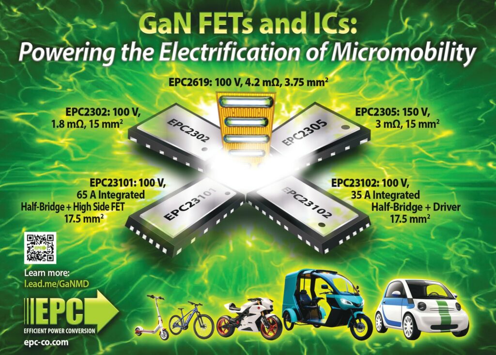
Gallium nitride
“There is a big macro shift with the power and cost of lithium batteries coming down,” says Alex Lidow, chief executive of GaN chip designer EPC and one of the original pioneers of the technology. “When that happens that goes right into the sweet spot of GaN with 26-48 V charging, 80 V and 96 V, and that is where GaN blows away the power MOSFET.
“The second thing is the motor drive and GaN has made huge changes there. Brushless DC motors have been the highest efficiency for battery systems at 20 kHz and down because of the MOSFET. It has this diode recovery that takes a while, and the motor has a dead time requirement of 500 nanoseconds (ns) for the MOSFET. The higher the frequency, the less inductance you need in the motor for the same amount of power, and that’s weight, so the motors are lighter.”
The dead time from the MOSFET is a counter force in the motor and takes away 5-6% of the power delivery to the motor. Then, as the motor drive shrinks, the electrolytic capacitors can be replaced with ceramic capacitors. The electrolytic capacitors traditionally are large and temperature-sensitive, and they are the first thing that fails.
“In some cases, the GaN motors are a quarter of the size of the MOSFET, and we routinely see them at half the size as a result of GaN,” says Lidow. These are also audibly quieter and have lower EMI.
“So far, the biggest successes have been at 100 kHz; all-ceramic capacitors, smooth motor drive with a smooth sinusoidal waveform – that’s the sweet spot. There’s a lot of work being done on motors for higher frequencies, and you see air-core motors at 250 kHz or 500 Hz. Where I think we will see those is in things that fly. A few of the eVTOL [electric vehicle take-off and landing] platforms have eight motors, each 200 A; the bus voltages are 96 V and that’s a good spot for GaN, so it’s not out of range,” he adds.

Lidow points to a laboratory in Torino, Italy, which is developing a large motor for eVTOL designs. “If it flies it’s going to be GaN,” he says.
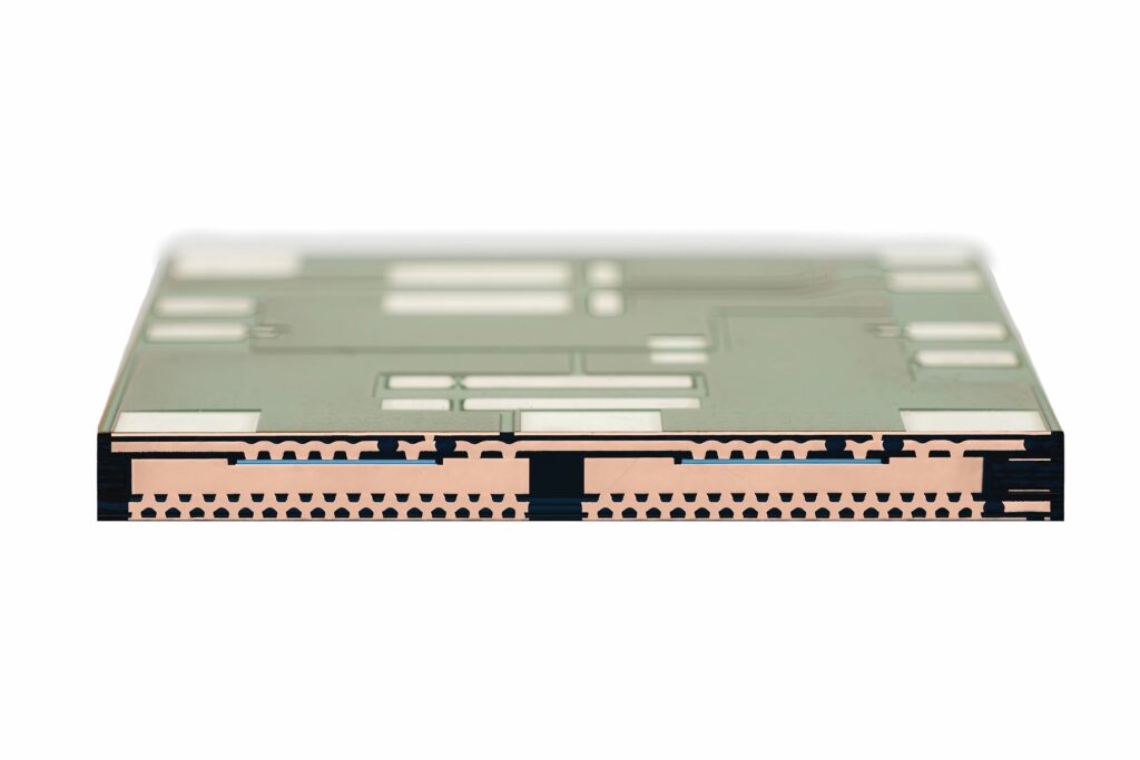
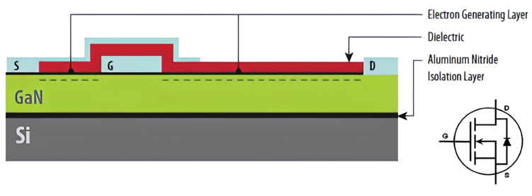
EPC developed enhanced-mode GaN HEMT transistors, which start with a thin layer of aluminium nitride (AlN), grown to isolate the device structure from the substrate. On top of this, a layer of highly resistive GaN is grown. This layer provides a foundation on which to build the GaN transistor.
Aluminium gallium nitride (AlGaN) is applied to the GaN, and this layer produces a physical strain, which attracts electrons to the interface.
This concentration of electrons is called a two-dimensional electron gas (2DEG). Further processing forms a depletion region under the gate, and metal layers are added to connect the three terminals, Gate, Drain and Source.
A cross-section of this structure is shown in the GaN transistor image (above). This structure is repeated many times to form a power device. The end result behaves in the same way as silicon MOSFETs.
“A native e-mode device at lower voltages looks just like a MOSFET except much faster, but that’s where the issues come in. In the motor there is the isolation, and there is a rule of thumb that you can’t switch the motor winding faster than about 10 V/ns because then the insulating resin tends to accumulate charge and breaks down, plus at high frequencies there have been problems with the bearing getting pitted from sparks,” says Lidow.
“While 10 V/ns for a 48 V motor drive is not a limitation, for a 800 V drive that’s 80 V/ns, so at high voltages there are problems with high frequencies. This can be addressed with multi-level drives. When you do that you only have the switching losses of the lower-voltage levels, so there would be eight segments for an 800 V motor. While this is more components, the GaN devices are significantly lower cost,” he explains.
A project at the University of Bern and the University of Texas at Austin has shown that the sweet spot for driving an 800 V motor is with 200 V devices for the power density, rather than cost, and these 200 V devices are mass-market. However, the multi-level design needs more isolators with multiple outputs.
“GaN is more reliable than silicon and that is becoming more widely accepted,” Lidow says. “The wide bandgap means it is far less sensitive to temperature effects. This means these devices last a long time and are more reliable at operating temperatures than room temperature, so the wear-out mechanisms are so much less.”
(Image courtesy of EPC)
GaN Systems/Infineon
Infineon’s GaN semiconductors are highly efficient for power conversion in the voltage range of up to 600 V. The CoolGaN 600 V GaN HEMT family uses an enhancement-mode design, based on the hybrid-drain-embedded gate-injection structure, which provides the highest level of robustness.
The HEMT devices can operate at high switching frequencies without compromising efficiency. Many enhancement-mode GaN HEMTs also add a diode to emulate a typical, insulated MOSFET gate.
The CoolGaN Integrated Power Stage (IPS) family is available in various configurations, including single-channel and half-bridge. While the half-bridge configuration combines two 600 V GaN power transistors with dedicated gate drivers in small-outline 27-pin and 28-pin packages, the single-channel setup uses only one 600 V GaN power transistor merged with tailor-made GaN drivers in a 21-pin package.
GaN Systems, now part of Infineon Technologies, also developed an enhancement-mode GaN-on-silicon power transistor. This implements a patented Island Technology cell layout for high-current die performance and yield, and it has attracted significant interest in automotive designs. This is coupled with custom packaging called GaNPX, which enables low inductance and low thermal resistance in a small package with a bottom side cooled transistor that offers very low junction-to-case thermal resistance.
(Image courtesy of GaN Systems/Infineon Technologies)
GaN depletion mode
The D3GaN (Direct Drive D-Mode) power switch, developed by VisIC Technologies, integrates a patented, high-density, lateral GaN power transistor into a ‘normally-off’ product with extremely low RDS(on).
The 650 V D3GaN technology has been implemented into an isolated, high-power package that includes integrated safety functions to ensure safe operation during system start-up and shutdown, while having no impact on the switching performance of the GaN transistor with an RDS(on) of 22 mΩ. This package has a small footprint of 19.7 mm x 13.6 mm, including the gull-wing leads, with top-side cooling for a heat sink specifically for EV designs.
The d-mode approach is also used by Transphorm.
The 2DEG is an incredibly fast channel that spontaneously forms at the interface between the GaN and a thin AIGaN layer. Its electron density is among the highest naturally occurring in semiconductors. It also offers high mobility, at 2000 cm2 /V·s, which is twice that of state-of-the-art silicon (Si) and silicon-carbide (SiC) devices.
This 2DEG channel at the AlGaN/GaN interface forms spontaneously with no need for external gate bias, so the device is normally-on and needs a negative gate bias to deplete the channel and turn off. It is a depletion mode (d-mode) device, but power electronic systems need normally-off devices for fail-safe operations.
The question then is how to make the lateral GaN HEMT normally-off. This is where cascode and e-mode technologies part ways. In the cascode technology, the GaN HEMT is untouched and the 2DEG channel is free to maximise its unparalleled combination of high mobility and charge density.

Transphorm’s cascode approach pairs the GaN HEMT with a low-voltage, normally-off Si MOSFET to achieve normally-off operation. This gives a positive threshold of 2.5-4.0 V, depending on power level, topology and system architecture.
This pairs the normally-on GaN HEMT with a highly reliable, highly performant, normally-off, low-voltage Si MOSFET in a cascode configuration. This ensures fail-safe, normally-off operations and is backward-compatible with today’s silicon technology.
Silicon carbide
With silicon carbide it is the material that is key, rather than the structure of the devices. Some are built on an engineered silicon wafer with a layer of insulator (silicon on insulator, or SOI) on the surface. These are now moving from 150 mm- to 200 mm-diameter wafers to increase the volume of devices that can be produced, reducing costs.
Others use silicon infused with carbide throughout. This creates a material that is as hard as diamond, making it more difficult to work with, but with better thermal and electrical characteristics, especially for trench structures. However, these devices struggle with the move from 150 mm to 200 mm for higher-volume production.
With a SiC-based MOSFET, the RDS(on) resistance only moves by a factor of around 1.13 between 25 C and 100 C, but with a typical, Si-based MOSFET such as the CoolMOS C7 from Infineon, it changes by a factor of 1.67. This means the operating temperature has much less of an impact on power loss and can therefore be much higher.
The cascode approach is also used with SiC devices alongside silicon MOSFETs for lower-power applications. Various devices developed by UnitedSiC and now Qorvo combine a junction FET (JFET) with a specially-designed silicon MOSFET with versions at 650 V, 1200 V and 1700 V, and currents up to 120 A. The advantage of this approach is that the cascode devices can be used with existing gate drivers and can be a drop-in for existing designs, delivering a lower RDS(on).

The future
The world of power semiconductor devices is shifting from silicon to wide bandgap materials. Device-makers are aiming to make the transition as simple as possible, using the same gate drivers as silicon. But the use of WBG devices is also opening up higher-frequency operation for smaller magnetics and smaller, lighter power designs, particularly in DC-DC and AC-DC e-mobility applications.
With GaN and SiC technologies maturing and coming down in price, adoption is growing, and the technologies are increasingly dominating the design and development of e-mobility powertrain and power systems.
Click here to read the latest issue of E-Mobility Engineering
ONLINE PARTNERS

