


Onboard Chargers
(Courtesy of VisIC Technologies)
EV users who need to prioritise safety and running costs should look to onboard chargers. Rory Jackson examines the engineering and technology inside them.
The route forward?
The viability of electric and plug-in hybrid vehicles depends on how quickly, efficiently and safely their battery packs can be recharged. At the moment, the charging times are as much of a bottleneck on the wider adoption of EVs as their range limits.
By and large, EV charging architectures can be divided into two categories – onboard charging systems, and ‘off-board’ fast DC charging stations.
Incorporating onboard chargers are seen by some end-users as a key limiting factor in EV recharge times. The hours taken to charge a battery can be calculated by dividing the energy storage (kWh) by the kilowattage of the charging componentry, and a 6.6 kW onboard charger will only deliver as much power as its rating indicates, even if a 22 kW AC station has been plugged into it.

But while some would therefore see fast-charging DC stations and connectors – in which high-power stationary AC-DC inverters are installed on the ground instead of the vehicle – as vital to reducing EV downtimes, the high charging currents associated with this approach inevitably harm the electrode materials of the batteries and shorten their lifespans. That drives up pack replacement rates and thus the costs of owning and operating battery EVs.
The high currents of fast charger stations can also cause issues such as lithium plating, in which lithium ions are deposited on the battery anode surfaces instead of between the layers of graphite. That not only weakens the performance and lifespan of the battery, it can increase the risk of short-circuiting and fires.
Using an onboard charger should therefore be the widely preferred option for users who are conscious of safety and running costs. These systems can be designed and optimised to improve the efficiency, convenience and performance of e-mobility platforms.

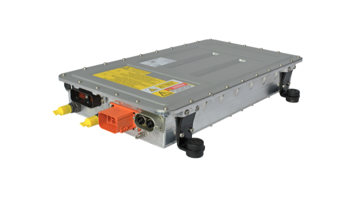
(Courtesy of NetPower)
Unidirectional onboard chargers
The onboard charging process starts when a Level 1 or 2 charging plug is connected to the input on an EV. These plugs are the most common format, and provide AC power, although the EV’s energy storage must be charged using DC power.
The conversion process from the grid’s AC to the DC required by the vehicle has a few key stages and corresponding components. Also, galvanic isolation (preventing unwanted current flow by direct conduction) is critical between the vehicle’s battery and the charging outlet in case there is a short-circuit or similar type of failure in the vehicle, to prevent damage to the ground power station. These two requirements are largely what dictate the kind of onboard charger architecture.
If we consider the power outlet as the starting point of the process and the vehicle battery as the end, the first stage is the power factor correction (PFC). This refers to the rectification of AC power into DC, as well as the additional goal of keeping the power factor – the ratio of real power absorbed by the load to the apparent power moving through the circuit – as high as possible, as it directly improves the efficiency of power transmission.
Once the PFC has converted the AC power into DC, the battery charging profile and state of charge (SoC) must be considered and accounted for. Every EV battery will have a variable voltage range: a light commercial EV might, for example, use a 220 V DC input at 0% SoC, while at 100% it could be around 450 V.
The onboard charger must be capable of changing the DC voltage output and current levels according to what the battery needs, in order to recharge it without overvoltage, undervoltage or related issues occurring. The circuit also requires a layer of galvanic isolation to prevent electrical shocks and damage, as mentioned (as well as helping to suppress electrical noise).
Therefore, the next junction in the onboard charger is usually an isolation transformer, many of which use discrete magnetics with handwound coils. These though are being surpassed in terms of reliability by planar magnetics, in which the windings and coils are embedded at the circuit level, enabling greater efficiency in compact packages.
The next stage can be referred to as the isolated DC-DC stage, as the fixed DC input from the PFC must be galvanically isolated and converted to the required DC output level. A few different converter topologies have been proposed, but two in particular stand out in terms of popularity.
One of them uses a ‘full bridge’ DC-DC architecture. This involves something of a roundabout approach: the DC input from the PFC rectification is inverted into AC (typically by four bridge-connected transistor-based switches) and that current is then applied to the primary end of a transformer, which will have been selected to step it up or down as the battery needs. At the secondary end of the transformer is a rectifier to then convert the transformed AC back to DC.
This approach is inherently wellsuited to galvanic isolation, given the absence of an electrical field between the transformer’s primary and its secondary (as it contains a magnetic field instead), and there are no limits on the conversion ratio. Also, the stress of charging is spread across four transistors, which is useful for highvoltage inputs.
For switching, however, having four transistor devices – typically MOSFETs, as well as at least two diodes – is costly for DC-DC architectures. That, as well as the need for other components such as ‘high side’ gate drives, adds design complexity and is an unnecessary complication for the lower input voltages involved with slow ‘trickle’ charging or for typical public charger stations rated to 120 or 240 V AC.
As publicly available charging outlets with voltage supplies above 400 V AC become more widespread, the full-bridge converter could become increasingly advantageous for onboard charger designs. However, the converters tend to be inherently more prone to switching losses than single ended converters of similar ratings, so the choice between the two might come down to priorities between costefficiency and energy efficiency.
LLC half-bridge converters, which use two inductors and a capacitor (as signifi ed by the two ‘Ls’ and single ‘C’), are the other of the most popular DCDC topologies for onboard chargers. These offer a lower component count than full-bridge types, as well as a higher maximum effi ciency level, as power is delivered from the transformer primary to the secondary almost 100% of the time.
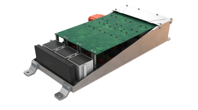
(Courtesy of Bel Power Solutions)
Bidirectional onboard chargers
Bidirectional charging represents the most advanced topology of onboard charger, and a range of manufacturers and users are looking to implement it.
While EV components are continually becoming more efficient, the proliferation of charging stations is predicted to place severe strains on the power grids of many nations. That could cause sharp rises in power outages or greenhouse gas emissions.
To reduce the burden on the grid, bidirectional onboard chargers could allow EV batteries at full charge to be discharged to a lower SoC (which would also help their lifespan), returning power to the grid when not needed. And with more buses, trains and other vehicles integrating solar cells, such EVs stand to replenish ever-higher quantities of the energy they take from the grid.
One of the problems is that most onboard chargers use boost (or ‘passive’) PFC architectures, which incorporate a passive diode bridge for rectifying AC into DC. This approach is simple and reliable, but it is not bidirectional.
A conventional boost PFC tends to use around four low-frequency diodes, one high-frequency diode and one high-frequency switch. By comparison, a ‘totem-pole’ PFC system uses two high-frequency switches – which will be SiC or GaN devices rather than silicon IGBTs or MOSFETs used by boost PFCs – and is inherently bidirectional.
The totem-pole PFC is one of the prominent architectural approaches to developing bidirectional chargers. By relying on GaN or SiC transistors rather than diodes for high-frequency applications, it offers higher power densities and effi ciencies than other PFC topologies.
These benefits come as a result of the better thermal performance, and lower switching and conduction losses of GaN and SiC compared with silicon IGBTs. The totem-pole PFC also avoids the conduction losses inherent in the front-end diode bridge rectifi er used by conventional boost PFCs. More and more developers are therefore looking to adopt totem-pole PFC designs.
Also, a bidirectional current fl ow must be designed into the transformer to support bidirectional charging. Dual active bridge (DAB) converters are perhaps the most promising topology for soft-switching, high-voltage bidirectional DC-DC conversion.
The DAB topology incorporates eight switching devices – twice as many as full bridge – as well as a high-frequency transformer, an energy transfer inductor and DC-link capacitors. Perhaps most important, they are symmetrical in design, with the primary bridge (at the voltage input) and secondary bridge (at the voltage output) being identical. That enables power to fl ow from the vehicle battery, back to the PFC and into the charging station port.
DAB converters also have the potential to reduce conduction losses and output capacitances, the latter of which dictates how high the switching frequency can rise.
Simulation and testing
The PCB design layout has important consequences for the performance of onboard chargers.
Having an efficient transistor is crucial, and a growing number of manufacturers are considering upgrading from their standard silicon IGBTs to SiC or GaN transistors. But if the PCB is poorly designed, the returns from investing in these new technologies (such as lower switching losses and higher switching frequencies) will be lost.
For example, a poor PCB board design for high-frequency applications such as EV onboard charging will suffer electromagnetic emissions or interference, resulting in losses at the transistor level.
Software such as Ansys Q3D and similar products can help immensely here though. These will generate computer simulations of EM emissions on a PCB layout that has been exported to the program, enabling fi nite element analysis to locate and extract all the parasitic EM losses across the board so that the charger’s internal layout can be optimised before manufacture.
Various power testing systems for prototypes or series production are also available for measuring voltages and currents. And as the power rating for transistors increases, new sensing solutions and probes have to be developed.
For example, using an optical fibreisolated differential probe can give far more accurate voltage readings for high-frequency switches than standard differential probes using copper for data readings. However, they can also be cost-prohibitive, and a probe with lower bandwidth might be more appropriate for a lower duty charger.
Other high-accuracy power analyser and meter systems are available for testing onboard chargers’ power efficiency, to precise measurements within 0.05% margins of error and at frequencies of up to 1 MHz. That is critical for high-end manufacturers looking to take their systems from 94% to 95% efficiency or more.
Power semiconductors
As all-new EVs are developed and the rate of electrifying existing fuel vehicles grows, power transistors have risen enormously in prominence and importance for powertrain engineers, and the ways they are connected and used are evolving rapidly.
Those engineers have started demanding ever-higher performance parameters, often at lower prices and without needing more operating power than the semiconductors in their old ICE vehicles used.
For the past several decades, the standard for semiconductor devices in high-voltage power supply switching applications was – and to a great extent, remains – the silicon IGBT. In the 1980s or so they gradually took over the high-voltage space from MOSFETs, which generally proved better suited to lower power switching applications, since IGBTs proved easier to control and better at efficiently and safely handling high current loads.

Despite these advantages and their overall robustness, however, silicon IGBTs are limited in terms of overall performance – specifically, in their maximum switching speeds, as well as minimising switching losses and also of conduction losses (which stem from voltage drops and current losses in the form of heat).
However, new technologies have appeared as a result of advances in materials science. Previously, silicon transistors manufactured on silicon substrates were the sole option, but now SiC-based devices manufactured on SiC substrates, and GaN transistors manufactured on silicon substrates, are competing here.
GaN and SiC are wide-bandgap materials, meaning the required energy for an electron to move from the top of the semiconductor’s valence band to the bottom of its conduction band is generally higher than one or two electron volts (eV). SiC ranges from roughly 2.3 to 3.2 eV, and GaN is about 3.4 eV (compared with silicon’s, which is roughly 1.12 eV). That gives SiC and GaN relative advantages in high-power and high-frequency solutions.
GaN in particular offers an inherent advantage in electron mobility, typically measuring 1500 cm2 /(V.s) – square centimetres per volt-second – compared with 900 cm2 /(V.s) for SiC and 1400 cm2 /(V.s) for silicon. This parameter typically means that, with transistors made from all three materials in equivalent size and shape, and all other controllable parameters being equal, the GaN device will have the lowest switching losses.
Also, developing systems for onboard chargers means engineers have to consider how these different materials handle high currents. For such applications, low resistance is critical, otherwise the charging process will induce high losses, and the architecture of GaN devices is typically geared towards low resistance in a superior fashion than in SiC and silicon devices.
These advantages stem from the lateral-form structures that suit the construction of GaN devices. Inside each transistor enclosure is an integrated circuit called a ‘die’, which consists of a block of semiconductor material on which the functional circuit has been fabricated. More often than not, in GaN transistors the junctions run from one side of the die to the other – as in laterally.
In addition, the typical architecture of a GaN transistor includes a ceramic layer of aluminium nitride (AlN) underneath the GaN die, between which is a nanometrethick layer of two-dimensional electron gas (2DEG) that serves as an ideal channel for rapidly transporting electrons. The flow of electrons through this channel is much faster than in silicon or SiC architectures.
In silicon and SiC transistors, electron gas structures cannot be formed, as they lack the material properties of GaN that enable 2DEG formation, so the conduction runs vertically, from the top to the bottom of the die.
That has important architectural implications for onboard chargers. The typical die for an EV power electronics module consists of hundreds of transistors packaged into its integrated circuit, compared with thousands to several thousand millions in a CPU. In order to handle higher current, more and more transistors must be built in parallel inside to reduce the resistance.
When more and more transistors are assembled together in this way, however, their capacitances are aggregated within the die. That increases switching losses when trying to handle increased current, particularly for silicon and SiC devices.

The lateral structures of GaN, on the other hand, are less prone to these kinds of losses (meaning more efficient charging), nor do they need to be paralleled, and so can handle higher and higher switching frequencies. With a greater switching frequency, the power conversion density is increased (meaning faster charging).
Increasing the switching frequency also means that the number of passive components, such as capacitors or inductors, in the onboard charger can be reduced.
For onboard chargers working upwards of 6.6 kW, it is important to be able to handle a lot of power while curbing the passive component content of the system’s architecture. Not only does that save on the material and component costs of onboard chargers, it does away with the need to build exponentially bigger and more unwieldy modules, which can quickly become impractically oversized for integration in all but the very largest commercial EVs.
Additionally, high-current PFC stages are often designed with ‘hard switching’, which entails significant switching losses (although they can be reduced by using SiC, and further so with GaN). With an isolation transformer, however, the circuit can be designed to perform ‘soft switching’, which means that such devices will experience considerable reductions in switching losses – perhaps around 90% less than hard-switching systems – and therefore much higher efficiency.
For example, the standard for EV PFC switching frequencies tends to be around 67 kHz for silicon and SiC in high-power vehicles, while some GaN soft-switching PFCs have been known to be double that. For the DC-DC stage, switching frequencies tend to run from 150-200 kHz for silicon systems, or up to 1 MHz for GaN transformers.
Transistor design
Improving efficiency has two key consequences. First, a higher proportion of the power from the grid is transferred to the battery, with lower losses and reduced burden on the grid. Second, the manufacturer of the charger and EV can worry less about cooling.
Inefficient systems generate more heat, so more heat sinks and perhaps a more extensive system of fans are needed. The system design might even need a liquid coolant framework, making the overall powertrain more expensive, bulkier, heavier and more power-hungry.
The thermal characteristics of power transistors are such that they all have to be cooled – they are not designed inherently for thermal transfer. It is also important to consider the transistor’s packaging, as that dictates to a large degree how efficiently the transistor can be used.
Among transistor manufacturers, a lot of modelling and design work typically goes into determining the optimal way to achieve that. It must be done without driving up the cost while still providing electrical isolation. For example, diamond is a very thermally conductive and electrically insulating material, but machining it into every transistor would be prohibitively expensive.
Typically, a thermally conductive material must be placed between each transistor and connected to a heat sink or cooling plate. The use of AlN, however, can transfer heat efficiently while also providing electrical isolation, and designing it into the transistor package’s architecture improves the efficiency of heat transfer.

That is one reason why GaN transistors designed in this way do not have to be paralleled for an onboard charger. The improved heat transfer through the use of AlN helps reduce switching losses further, so each GaN device can handle more power than an equivalent silicon device.
However, that also makes it challenging for some companies to adopt GaN, as the material’s many different properties compared with silicon mean it cannot be applied as a simple drop-in replacement. New onboard chargers must therefore be re-architectured from scratch to achieve sufficient return on the cost of investment.
A range of other ceramics can also serve this purpose, including silicon nitride or aluminium oxides, but AlN provides the highest thermal conductivity and thus the lowest heat resistance.
Some power modules will typically incorporate a large ceramic substrate with many transistor dies mounted on it in varying configurations. Some manufacturers have now taken that approach down to the device level, which has been found to improve the overall efficiency in terms of energy, thermal and weight at the resulting module level.
Companies should also consider the difference between E-mode and D-mode transistor designs, ‘E’ meaning ‘enhancement’ and ‘D’ meaning depletion. The terms stem from the construction of the transistor gate.
Every MOSFET has a ‘drain’, a ‘source’ and a ‘gate’, (while every IGBT has an ‘emitter’, a ‘collector’ and a ‘gate’) with the former two terminals carrying current flow, and the gate terminal’s voltage controlling whether or not current flows between them. The chemical construction of the gate determines whether the MOSFET is a D- or E-mode device.
An E-mode device is inherently set to ‘off’, and is therefore not conducting; D-mode devices are ‘on’ and conducting by default, so they need additional circuitry inside to actively switch them off, which adds a small amount of weight and complexity. An onboard charger using D-mode transistors could thus be more costly than one using E-mode devices.
Manufacturing high-voltage E-mode transistors inherently means having ‘defects’ such as a p-type doped GaN cap layer in their gates, however, making it harder to certify them according to automotive industry qualification standards. While several D-mode GaN transistors have been certified, 600-650 V E-mode GaN devices have not.
Control systems
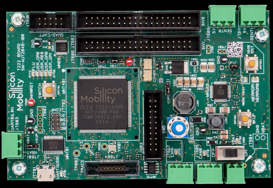
(Courtesy of Silicon Mobility)
When plugging the charging outlet into the onboard charger, a well-designed controller is key for receiving and processing the charging data and controlling the systems involved, as improvements in the hardware and software for control can enhance the charger’s efficiency by up to 10%.
Naturally, the electronic control unit for the charger must be designed with the correct data inputs and control outputs for charging systems. This includes being able to closely track critical variables in the PFC and DC-DC converter, such as inductor current, load current and voltage, and overvoltage or undervoltage conditions.
Furthermore, as chargers handle larger quantities of power and are programmed for tighter control and greater safety, control algorithms need to become increasingly complex in order to accurately regulate output voltages.
With SiC and GaN transistor devices increasingly pushing switching frequencies up to the hundreds of kHz or even to MHz speeds, processors have to be used that can run the gate drivers at matching speeds, as well as handle the complex control algorithms and critical information stream from the charger stages.
The choice of control system in power converters tends to come down to microcontroller units (MCUs) or digital signal processors (DSPs).
The former, being multi-core ICs, tend to be optimised for flexible subsystem integration. That means they can quickly be loaded with a wide range of software algorithms, lending them well towards controlling PFCs, DC-DC converters and the charging station at the same time.
However, they are not necessarily adapted for critical factors specific to electric powertrains, particularly for high-frequency calculations. DSPs on the other hand are designed to be much faster for integer mathematics, floating-point operations and other numerical data-focused processes than MCUs.
Microcontrollers can be loaded with software designed to perform these functions, but they can still face bottlenecks in terms of how quickly the software can process complex control tasks for high frequency switching, often being limited to between 10 and 20 kHz. As a result, DSPs have become the standard for many power converters’ control systems, and there are also some designs based on field programmable gate arrays (FPGAs), as they are architecturally similar to DSPs.
Further creative routes to precise high-frequency charger control can be found throughout the industry. One approach takes a combination of a standard CPU with a flexible logic unit (FLU), which works in a similar way to an FPGA. It features programmable logic designed for autonomously acquiring highfrequency data inputs as well as handling the high-frequency control algorithms required for EVs. Automotive constraints and safety requirements are also accounted for in the design process.
The algorithms in such a system can also feature independent control loops for each phase of the charger, providing operational efficiency and the capability for soft switching in PFCs and DC-DC conversion. Soft switching requires more robust and complex algorithms than hard switching – if an MCU were to try to control soft switching it would almost certainly fail and generate impractical levels of heat in the attempt.
On the other hand, FPGAs can easily be affected by ‘single-event upsets’ because of the sensitivity of their components to ionisation. Specialised safety functions must therefore be included in their operational algorithms, and in some cases an external monitoring MCU is added. Furthermore, the size of an FPGA matrix makes them time-consuming and costly to load and test.
A combined FLU-CPU system improves over the inflexibility of MCUs and FPGAs in terms of speed and versatility respectively, as it is tailored for onboard charger (and other EV power converter) manufacturers and can enable switching speeds for IGBTs and MOSFETs to improve to the point where they are comparable with SiC performance levels.
That in turn could lower the material cost, system complexity and weight for onboard chargers, as it means EVs could continue using IGBTs and older technologies by just swapping in a better controller instead of having to integrate newer ones.
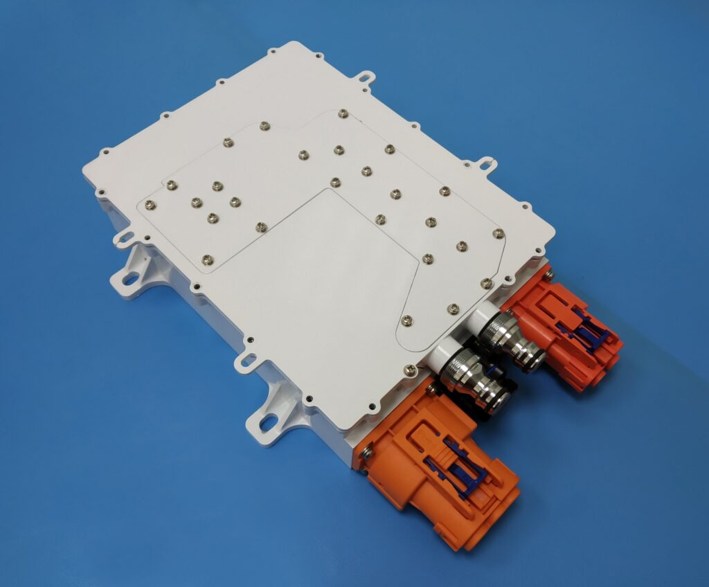
(Courtesy of VisIC Technologies)
Conclusion
With GaN, SiC, and new control architectures poised to enable major gains in energy efficiencies, future EV designs will evolve in response.
Such changes are likely to include bidirectional onboard chargers and more rooftop solar panels to ease the pressures that EVs pose to national grids, and battery packs with higher energy-toweight ratios that will make it easier to fit them into a given space and volume in a vehicle chassis.
Acknowledgements
The author would like to thank Elijah Bunin of VisIC Technologies, Khaled Douzane and David Fresneau of Silicon Mobility, Tim Skerra of Innolectric, Frank Vondenhoff of Bel Power Solutions, and Dr Yimin Jiang of NetPower for their help with researching this article.
ONLINE PARTNERS
