


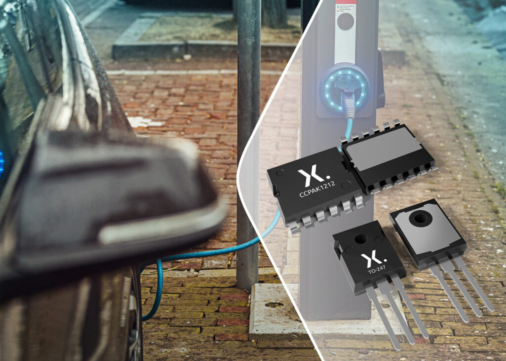
Power electronics

(Courtesy of Delphi/BorgWarner)
Nick Flaherty explains the three types of switching technologies for inverters and how to match them to a given inverter design.
Three-way choice
Power electronics is of course a key technology for e-mobility systems, and the development of their components is a vital part of the evolution of system designs. New technology is opening up opportunities to increase the performance of power systems, while improved efficiency is leading to smaller converters or more power from the same size. But cost – not just of the components but also of the converters and the rest of the power system – is a key consideration that is driving design decisions.
The heart of the power system is the inverter. As battery packs move from 400 to 800 V, to provide more power, so there is an increased focus on the performance of its switches.
The inverter relies on semiconductors that can switch quickly to provide a smooth AC waveform for the motor. That may need to be a perfect sinusoidal curve, but depending on the type of motor, there may be variations in the waveform that make the overall system more efficient. This requires a switch that can respond quickly – that is, has a fast frequency response – as well as a controller that can create such waveforms.
This speed of switching and degree of controllability forms the core of the power design of an e-mobility platform. Higher frequency switching brings more efficiency and lower losses, giving fewer thermal issues and higher reliability.
Different types of switches offer different trade-offs in speed, maturity of the technology and cost. It is becoming clear that the three main contenders have comparable reliability, so designers have a range of options in the implementation of the power electronics. All three technologies use the same standard silicon fabrication techniques but have very different performance and requirements for the controller, also called the gate driver.

These switches can also be used in other areas of an e-mobility platform for power conversion. Hybrids are evolving to 48 V power distribution buses for models in 2022 and 2023, but they still need a 12 V supply for legacy systems, and switches that can operate at 200- 500 kHz reduce the losses in these systems.
There are also DC-DC converters and onboard chargers that need power conversion at 400 and 800 V. While higher frequency switching allows more efficient and therefore smaller designs, this also changes the way these parts of a platform can be designed. Custom integrated power electronic designs for example create ‘bricks’ that combine DC-DC converters, onboard chargers and auxiliary inverters.
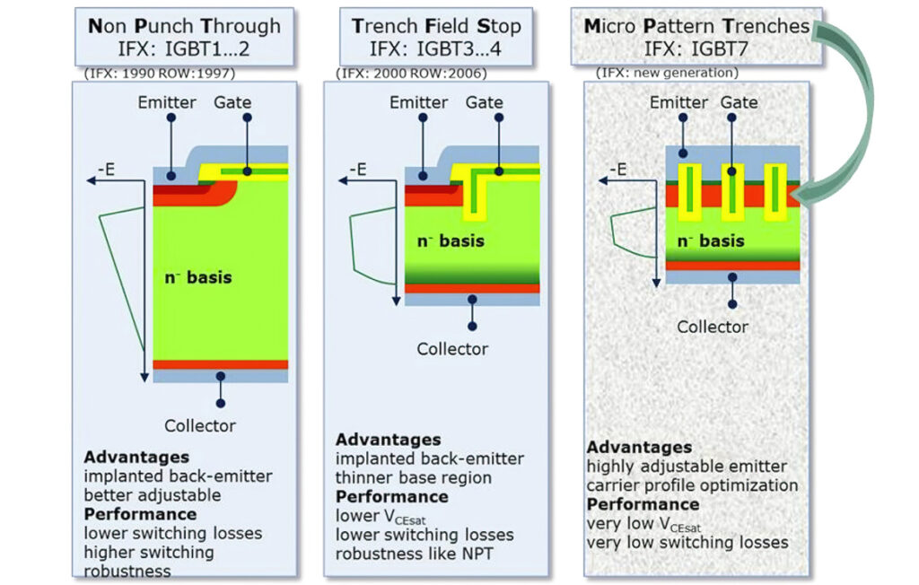
Silicon IGBTs
The most mature switching technology is the insulated-gate bipolar transistor (IGBT). This is a three terminal power semiconductor built on a standard silicon wafer, and can handle voltages from 650 to 1200 V, and as high as 1700 V. However, the switching speed is limited to around 15 kHz, although the switching speed is a balance between the current capability (which depends on the capacitance) and the resistance of the device, which varies with temperature.
The IGBT is a vertical, or trench, device, as the layers of the transistor are stacked on top of each other. This makes the chips cost-effective, as more of them can be fitted on a wafer compared with a planar design. The trench around the vertical transistor provides more isolation than a planar design and so allows higher voltage operation than other switch technologies – at 1200 and 1700 V.
While IGBT technology is the most mature, it is still developing, both in terms of performance and the ability to make the devices on the largest 300 mm silicon wafers for the lowest cost compared with the current 150 and 200 mm wafers.
(Courtesy of Infineon Technologies)
One development here is the Power2Power project in Europe, which includes 43 partners working on new silicon IGBTs with higher power density and energy efficiency. It aims to develop the first qualified technology for‑IGBTs above 1700 V‑on 300 mm wafers, as well as devices with a 200 C junction temperature.
That would allow a 20% increase in power density and‑50%‑longer lifetime. It could also provide a‑10% reduction of losses in inverter designs, particularly for electric trains, but the project will not deliver initial devices until 2023.
The planar approach by contrast has the transistor junctions spread out laterally on the top layers of the wafer. The manufacturing process is simpler but the larger devices means fewer of them can fit on a wafer, making a planar chip more costly.
That is an issue within the competition between IGBTs and one of the competing technologies, silicon carbide (SiC).
This is a wide-bandgap semiconductor, meaning it has a wider electron band gap than a silicon semiconductor. That allows the chip to carry more current and dissipate less heat when switching through a lower on-resistance, or RDS(on). The maximum saturation current is also a key indicator of performance for an IGBT.
While there is a natural focus on the RDS(on), another quantity known as the Figure of Merit also helps to determine the performance of power switches.
SiC switches
An SiC switch is generally a metal-oxide semiconductor field effect transistor (MOSFET). This uses an insulated gate to switch a semiconductor junction underneath.
SiC MOSFETs are moving from planar devices to vertical structures with a lower RDS(on) that can switch faster as they have lower losses; they are also more cost-effective.

However, there is a different form of SiC switch that can be dropped in as a replacement for an IGBT, and this is moving to a lower-cost vertical structure.
The Figure of Merit for an SiC MOSFET is the product of the RDS(on) and the gate charge, which is the charge that must be brought to the gate of the‑MOSFET‑to turn it fully on. That determines how quickly the device can switch and hence its frequency of operation.
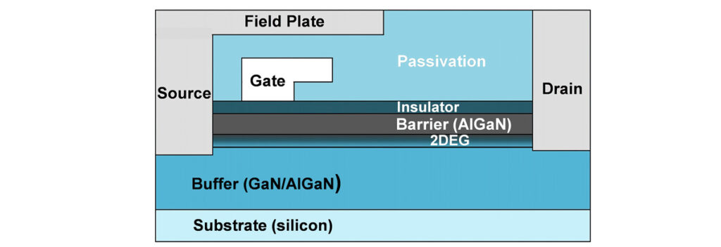
GaN switches
The use of a vertical or planar design varies again with gallium nitride (GaN), which is another wide-bandgap material. GaN devices use a different structure, called high electron mobility transistor (HEMT), and that has different implications for cost.
They are built on a standard silicon wafer with a layer of GaN added on top in a separate reactor. That tends to make the devices planar, as the GaN layer is a few nanometres thick. They behave in a similar way to silicon power MOSFETs but have switching speeds of up to 2 MHz.
There are two different technologies, depletion or D-mode, and enhanced or E-mode. D-mode provides a higher gate drive safety margin and gate drive noise immunity with relatively simple parallel operation, which is important for GaN inverters that use multiple levels in the bridge.
D-mode devices have an RDS(on) down to 8 m at 650 V and 200 A, while for E-mode devices it is typically 20 m. However, the two types have different design considerations.

A D-mode‑transistor is normally on‑and‑is switched off by a negative voltage relative to the drain‑and‑source electrodes; with an E-mode‑transistor it is normally off‑and‑is turned on by positive voltage applied to the gate. E-mode is a more common design approach for high-power designs such as an inverter, although there are more reference designs emerging for D-mode devices.
The manufacturing approach of adding a layer of GaN also opens up opportunities for integration, as ordinary silicon transistors can be built on a wafer before or alongside the GaN transistor in a standard process before going into the reactor. That allows the gate driver to be added in the same chip, avoiding the need for a separate gate driver.
Although a GaN chip may be larger and more expensive, the overall design can be smaller and cheaper than the alternatives. The dramatically higher switching speed also means higher efficiency and lower losses, reducing the amount of cooling needed and further reducing the weight and cost of an inverter, for example.
Vertical trench GaN transistors using thicker layers of GaN are also under development, but the challenge is to create these thicker layers with a crystalline lattice.
Wafers
There is also the issue of the wafers used to make these chips. IGBTs can be built on standard silicon wafers that are 200 or 300 mm in diameter, producing many thousands of devices. SiC wafers require an ingot of standard silicon to be infused with carbon at high temperature, creating a block that is almost as hard as diamond. That then has to be cut up into individual wafers, which can be costly.
With GaN chips, the additional stage is the reactor, which can accept any size of wafer. These have been added alongside standard silicon chip-making processes, making GaN devices more cost-effective than SiCs.
Inverter design
The fundamentals of IGBT inverters haven’t changed since they were commercialised in the 1990s. The gate drivers have become smarter, but fundamentally they consist of a three-phase bridge, the main difference being that SiC is becoming increasingly viable. The use of SiC is initially in supercar applications but electric motors are spinning faster as the materials allow them to have a higher tip speed so they need faster switching.
There is also an issue of audible noise. IGBTs switching at 5-10 kHz can be audible, but pushing the frequency up above the audible range to 12 or 15 kHz increases the losses. That means a bigger device is needed to handle the same power, but that creates more heat and thermal effects so it is less efficient, meaning shorter battery life and reduced range.
Traditional 600-1200 V IGBT devices driven by a single- or three-phase control signal were originally designed into industrial motors, which led to 400 or 800 V battery systems, as the semiconductor switches were already available. The limitation for the 400 V system is the current draw required for the power consumption. Once that exceeds 1000 A, the issue then is with the conductors, so above a power draw of 350 kW a move to an 800 V battery pack needs to be made.
Inverter designs based on IGBTs handling 300-800 A are now more than 98% efficient in 120 kW/400 V and 225 kW/800 V implementations. They have an operating temperature of -40 to +125 C, with coolant temperature to 70 C and 10 litres/minute flow rate, and are built in lightweight aluminium casings for electric aircraft designs.
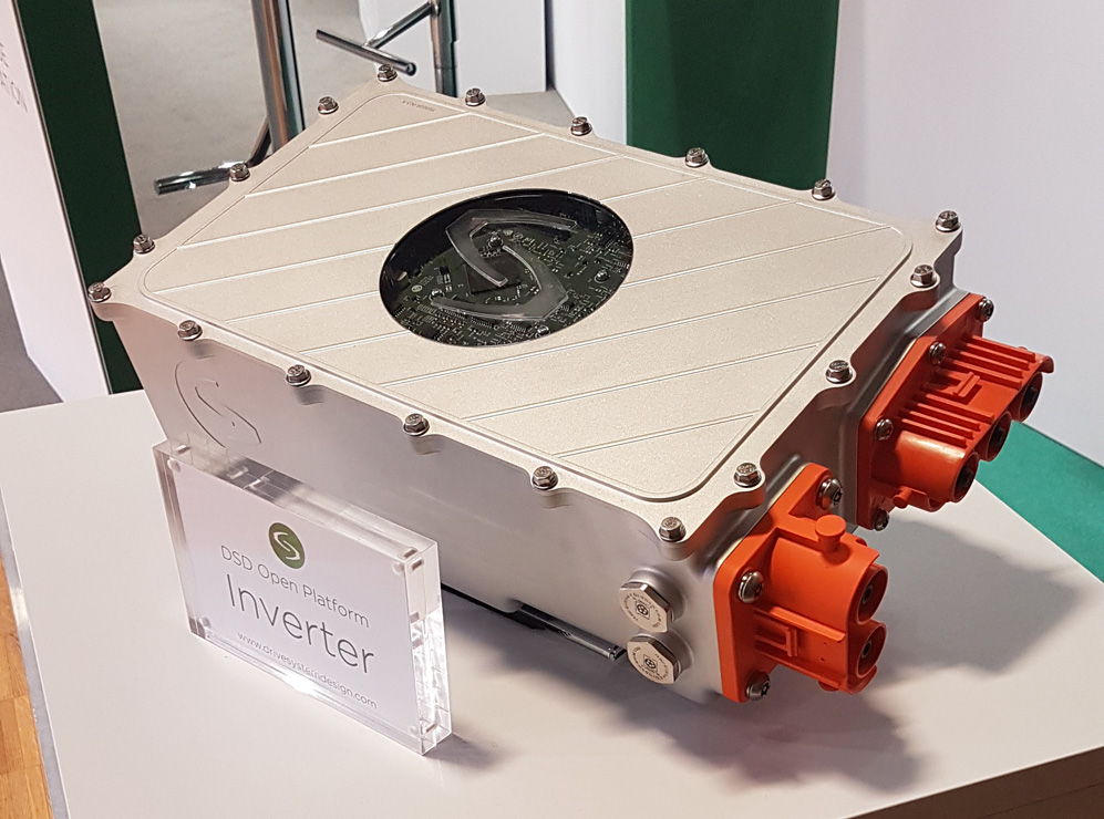
(Courtesy of DSD)
However, the need for faster devices and an 800 V pack is not just a technical one. An EV with reasonable acceleration that can drive at national speed limits is perfectly possible with a 400 V pack and 200-300 kW power, using 650 V IGBT, SiC or GaN devices. When there is a demand for 800 kW in a car with acceleration of 0 to 60 in 2 or 3 seconds then 1200 V devices are required, which then means using IGBTs or SiCs.
Moving to SiC cuts the losses in an inverter by 70% and the size by 60%, say system makers planning to include the technology in new designs in vehicles in 2022.
There is a lot of debate over the drop-in replacement of an IGBT with an SiC switch. One argument is that simply dropping in an SiC switch doesn’t give much of a performance advantage for the added cost; to gain an advantage requires modifying the gate driver for higher frequency switching that can provide a more accurate switching waveform. However, that is possible with existing programmable gate drivers, which can boost the switching frequency above the audible range without the resulting losses of a larger IGBT.
One supplier is using a different approach, putting a silicon MOSFET in the same package as an SiC junction FET (JFET). The MOSFET acts as a controller for the JFET, which is simpler and cheaper than an SiC MOSFET and allows existing IGBT gate drivers to be used. These can be used at switching speeds of 150-200 kHz to improve the efficiency of inverter designs.
Every Watt saved in efficiency saves a Watt in cooling, so there is a magnifying effect in reducing losses, which gives a lighter design and longer range.
A D-mode GaN-based 100 kW inverter reference design can be adapted for 800 and 900 V power buses. Its estimated peak efficiency can reach 99.3% with a 40 kHz switching frequency, owing to the low switching losses of the GaN devices.
One inverter using these devices measures 26.9 x 21.4 x 3.5 cm‑with a liquid-cooled heat sink. The power density is 50 kW/litre‑including the liquid cooling, and the inverter weighs 2.5 kg.
IGBT module design
The HybridPACK DC6i combines six IGBT switches in a module with an emphasis on the thermal management for inverter designs.
One of the latest IGBT modules has the same footprint (7.2 x 14 cm) as the previous family but with a later generation power switch. These switches use micro-pattern technology to deliver a power output that is more than 50% higher than previously, as well as a voltage of 750 V, a short-term extended operation temperature of 175 C and high short-circuit ruggedness. The design trade-off between switching and conduction losses is optimised for a real world driving cycle with low light-load power losses.
The module has six screw connectors to the DC-link capacitor, compared with two in the previous family. This enables a low-inductance design with a stray inductance of 15 nH. A patented direct cooling wave baseplate provides heat dissipation with a thermal resistance from the IGBT chip junction to the fluid of 0.17 K/W.
Press-‑it pins and additional guiding elements enable gate driver board mounting in a few seconds, compared with traditional selective soldering of more than a minute.

Gate drivers
Modern driver chips are fully programmable, so the profile of the charging voltage for the gate can be varied via a CAN network link. This link allows the gate waveform to be modified in real time, optimising the switching for the type of motor being used.
Gate drivers are now flexible enough to support IGBT and SiC MOSFETs, although they tend to be produced by the maker of the switching chips to match the performance required of the inverter and the motor it is driving.
The inverter design tends to be coupled with a specific motor, and there is a wide range of these for e-mobility applications that require different waveform profiles determined by the driver. The waveforms also differ according to the system to be used. The different motors, from inductive and permanent magnets to synchronous axial flux or transverse flux, have different ‘sweet spots’, and the gate driver has to tune the switching transistors, which are arranged in a bridge configuration.
The transistors are built in standard silicon to control the two sides of the bridge, the high voltage and low voltage. As a result, there is a need for isolation around the driver, which operates at 5 V, in a high-voltage environment of 400 or 800 V.
This isolation is often provided by an air gap – that is, a capacitative isolation, an inductor or using an optical coupler that converts the analogue signals from the driver into an optical signal and then back again on the high-voltage side. However, all these methods reduce the speed at which the inverter can be controlled efficiently.
Another approach is to integrate magnetic isolation into the driver package. This provides a much faster feedback loop, and so allows higher frequency inverter designs. It also eliminates the need for tantalum and electrolytic capacitors, which can be more costly or less reliable, and requires only one transformer secondary winding.
That reduces the PCB’s design to two layers, making it simpler and less expensive, and boosting the reliability as there are fewer components that might fail.
Packaging
Another key factor is the packaging, as it contributes to the resistance and capacitance of the switch, reducing the maximum possible switching frequency. One way to minimise these effects is to use an additional lead, meaning four-pin devices (also called Kelvin packages), which can spread the resistance and reduce the resistance and capacitance in the critical path.
Thermal issues are also critical with devices operating at 1200 V and switching up to 1000 A at high speeds.
This is driving the development of chip-scale packages (CSPs), which eliminate the lead frame that holds the chip in the package and connects to the pins. That enables a smaller package with better thermal conductivity that can be cooled on both sides. CSPs also support silicon IGBT, SiC and GaN devices.
However, CSPs are harder to integrate into an inverter, so they tend to be designed into a module with six transistors for a bridge for each phase. A three-phase converter would therefore have three modules.
Ideal-mode GaN
One major automotive chip supplier is developing a single 650 V GaN family for inverter and DC-DC converter designs. This family of chips operates in a different way from other GaN devices, called ideal mode.
(Courtesy of VisIC)
GaN chips are being used to reduce the size of inverter designs and boost the energy density (Courtesy of VisIC)
It is integrated with a programmable 2.2 MHz driver and safety controller. The integration of the silicon driver with the GaN switch in the same package monitors the temperature and any current surges. The chip can report the temperature and any faults to the system.
It is also intended to be a single device configured for multiple different applications in an EV, from a DC-DC converter to the onboard converter or the inverter. This simplifies stock management for electric car makers and gives economies of scale to drive the price down to compete with IGBTs.
Some of this comes down to its reconfigurability, by using one part for many different power designs in the vehicle. For example, it can be used in high-frequency designs from 500 kHz to 2 MHz for a more efficient onboard charger or DC-DC converter using a conversion topology such as a totem pole that gives more efficiency. This also allows the two functions to be combined into a single ‘high power block’ unit, reducing the overall complexity of the system.

The same chips can also be used in lower speed multi-level full-bridge topologies at 150-200 kHz for inverter designs, still five times faster than IGBT designs, with smaller heat sinks thanks to their higher efficiency. They can be programmed to provide different performance levels from the same inverter design for different e-mobility platforms, again reducing complexity.
Switching 5 kW in a standard small quad-flat no-lead package becomes possible by putting the silicon driver in with the GaN to provide the power in a small volume. This also adds the ability to monitor the current and temperature for early identification of any problems.
This integration has enabled inverter designers to move from liquid cooling to forced-air cooling, or from forcedair to convection cooling as a result of the higher efficiency.
Cascode GaN
Another approach to a GaN device mirrors that of the simpler SiC cascode devices, and is being used by another major automotive chip supplier.
Combining a HEMT GaN-onsilicon transistor with a low-voltage silicon MOSFET in a single package reduces the complexity of designs by allowing a simple silicon driver to be used but with a 15% performance improvement.
This comes from using a technique called through-epi vias to make a connection through the GaN layer to the back of the 200 mm silicon wafer. This reduces defects and shrinks the die size by around 24% compared with the first generation of such devices.
Using through-epi vias also allows a bottom connection on the device. That eliminates the ceramic shim that was needed in the first implementation, improving the thermal performance and reducing the cost.
A single ideal-mode 650 V GaN switch packaged with a controller can be used across a wide range of power designs in an EV
(Courtesy of Texas Instruments)
The first versions of this approach qualified for automotive use are aimed at 400 V DC-DC converter designs. They have an RDS(on) of 41 m, and have been used for a demonstration 85 kW inverter design. The parts are tested to 500 kHz for a DC-DC converter, while a traction inverter design runs at 20-30 kHz because of the need to minimise the EMI, although some are pushing to 40 kHz.
Packaging is a key element for automotive designs, and the device is initially being packaged in a standard TO-247 case. A copper clip surface mount packaging called CCPAK reduces the RDS(on) to 39 m by replacing the internal bond wires with copper clips, reducing parasitic losses and optimising electrical and thermal performance, and improving reliability. These CCPAK GaN FETs are available in top- or bottom cooled configurations to improve heat dissipation.

Future optimisations of the process and package will see the RDS(on) falling to below 20 m for 100 kW designs, and a third-generation technology will cut that to 10 m; 900 and 1200 V GaN devices are planned to support 800 V systems directly.
This third generation will focus on driving down the RDS(on) at 650 V to achieve a power of 150 kW in a 2 litre inverter with 10 m and 100 A switching. That matches anything coming from SiC.
Reliability
One issue raised about GaN in particular is the reliability of the devices. IGBT and SiC MOSFETs have well-established device structures and are built on substrates whose performance is well characterised. That is not the case with GaN though, which with its thin layer of gallium nitride on a silicon substrate has multiple potential failure mechanisms with the HEMT structures. The different modes of operation, E- and D-mode, also mean there are other failure mechanisms.
However, the technology has been under development for 20 years, and there are now billions of hours of test data for GaN devices of all kinds from multiple suppliers with different approaches to device operation.
The latest phase of test data for E-mode devices, phase 12, has taken a major step forward. Previously, a statistical model had been used to predict failure rates, and that was sufficient to achieve AEC-Q100 and AEC-Q200 qualification for the use of GaN devices in automotive designs. With the latest release, a physical model of device operation has been developed that matches the statistical data collected during development.
(Courtesy of Nexperia)
That provides enhanced confidence in the reliability of the data by predicting failure rates for voltages and temperatures, which may not have large amounts of test data.
The physics-based lifetime model with supporting evidence is shown to project the lifetime of an eGaN device undergate stress over all voltages and temperature ranges.
The model describes the dynamic RDS(on)effect in eGaN FETs derived from the basic physics of hot carrier scattering into surface traps. It is most useful for predicting lifetimes over all voltages and temperatures in more complex performance profiles. Using the model, a system has been developed to assess eGaN reliability over long term ultra-high dv/dt and di/dt pulse stress conditions.
The model’s accuracy has been tested with a study of thermomechanical stress under temperature cycling and intermittent operating life to experimentally generate lifetime predictions and guidelines for the selection of under fil lbased on key material properties.
Similarly, the developer of ideal mode devices has also been testing the technology in the field for more than 10 years. That allows AEC-Q qualification for 650 V devices.

As a result, the GaN chip suppliers are confident that the technology will overtake IGBT, offering higher power densities and frequencies with similar manufacturing costs after moving to vertical trench structures and integrated drivers.
However, SiC vendors see the options as so fragmented that there is room for IGBT for lower cost 400 V systems, SiC for 400 V and 800 V medium-frequency designs, and GaN for 400 V high-frequency, high-efficiency designs.
Conclusion
A common view is that GaN technology will be used primarily in the 400 V power bus because of its lower cost compared with other wide-bandgap technologies, and SiC is commonly used in the 800 V power bus for higher power applications. The 100 kW inverter reference design demonstrates that GaN technology can be used in 800 V power bus applications as well.
However, the low cost and continuing development of IGBT technology means it will continue to be widely used.
Acknowledgements
The author would like to thank Murray Edington at DSD, Chris Dries at UnitedSIC, Alex Lidow at EPC, Steve Lambousis at Texas Instruments, Jim Whitham at GaN Systems and Michael LeGo at Nexperia for their help with researching this article.
ONLINE PARTNERS

