


Improving power electronics
(Courtesy of QPT)
Switch gear
Nick Flaherty reports on how semiconductor r&d is leading to more efficient and powerful electronic switching solutions for e-mobility
Power devices for e-mobility come in a range of technologies to boost performance and efficiency. Insulated gate bipolar transistors (IGBTs) made from silicon have been the original power switch for decades; they are robust and low cost but can only switch at frequencies of around 10 to 20 kHz.
Silicon carbide (SiC) increases that frequency to 200 kHz, with lower losses and higher robustness than IGBTs but at a higher cost. Gallium nitride (GaN) is now emerging as a potential high-power switching technology, with operating frequencies of up to 20 MHz, but their robustness and the maximum voltage, or withstand voltage, have previously been a challenge.
SIC and GaN are both wide bandgap materials, where the higher bandgap compared to silicon gives higher electron mobility, leading to higher switching frequencies that in turn give higher efficiency and performance for power electronics designs.
Of course, engineers have been working on all three technologies to boost the performance of each one in different ways. IGBT developments are working on ever higher voltages – 1200 to 2000 V – while SiC is looking to a trench structure to fit more devices onto an expensive SiC wafer to bring down the cost.
GaN is intrinsically less expensive than SiC, using GaN layers on a low-cost silicon wafer. Designers are pushing up the withstand voltage of GaN, as the higher frequency is extremely appealing, although existing 650 V GaN devices are being used for 800 V inverters without having to go to 1000 or 1200 V.
This higher frequency, up to 2 MHz or even 20 MHz, is highly attractive for power electronics designs, as it allows the magnetics of converters to be reduced in size, cutting the weight and footprint of onboard chargers and even inverters.
The different technologies lead to different device structures and a range of implementations for power electronics. Bipolar IGBTs are the simplest, and share similar voltages with SiC MOSFETS. These are driven by voltages of about 5 V to switch them from off to on.
In contrast, GaN high electron mobility transistors (HEMT) devices have a very different structure, and come in versions that are normally off, also known as depletion mode or d-mode, or normally on, with enhanced mode or e-mode. These have different drive requirements and implementations.
However, these higher frequencies present challenges in designing the power electronics, so new techniques have been developed using machine learning to enable designers to exploit the advantages of GaN despite the design challenges.
(Courtesy of Infineon Technologies)
IGBTs
Infineon Technologies has completed a €74 million project to build 1700 V IGBT power transistors on 300 mm silicon wafers. The Power2Power project brought together 43 partners from industry and research in eight countries over the past 3 years to boost the voltage, reliability and robustness of the transistors for transport and heavy industrial applications such as battery systems and chargers for electric vehicles
For EVs in particular, the development boosts the efficiency of these devices to 98% with a 200 ºC junction temperature, taking on SiC directly. At the same time, the developments improves IGBT lifetime by 50% and cuts the cost of a drivetrain inverter by a third with 10% lower losses.
A follow-on project, called PowerizeD, is working on making the power electronics designs more digital.
Renesas Electronics has also developed new generation of IGBTs that reduce their size and power losses. Its AE5-generation IGBTs are built on larger, 300 mm wafers and achieve a 10% reduction in power losses compared to the current-generation AE4 devices, a power savings that will help EV developers increase the efficiency of the power electronics to increase EV ranges.
The devices are about 10% smaller than before while still maintaining high levels of robustness. Their design also improves performance and safety as modules by minimising parameter variations among the IGBTs to ±0.5 V. This provides stability when operating IGBTs in parallel, and means the modules do not have to be over-designed to accommodate device variations; they can also be used as a bare die in a module or in an inverter design, saving space.
The devices have a withstand voltage of 750 V with currents of 220-300 A for 400 V battery packs, and a withstand voltage of 1200 V and currents of 150-200 A for 800 V packs. This is 10% higher currents than previous devices in a smaller die size of 100 mm2 for the largest 300 A part.
They all have an operating junction temperature range from -40 to 175 ºC, allowing for higher temperatures in the inverter. As a measure of the robustness, the reverse bias safe operating area has a maximum current pulse of 600 A at the highest 175 ºC junction temperatures, and a highly robust short-circuit withstand time of 4 µs at 400 V.
There are a number of design enhancements to boost efficiency. The first is an increase in the saturation voltage to 1.3 V as well as a 50% reduction in the temperature dependence of gate resistance. This minimises switching losses at high temperatures, spike voltage at low temperatures and the short-circuit withstand time, supporting high-performance designs.
These advances reduce the inverter power losses, improving power efficiency by up to 6% compared to the current AE4 process at the same current density, allowing EVs to drive longer distances or use fewer batteries. The AE5 IGBTs have been used in a hardware reference design that combines the IGBT, microcontroller, power management IC, gate driver IC and fast recovery diode for an inverter.
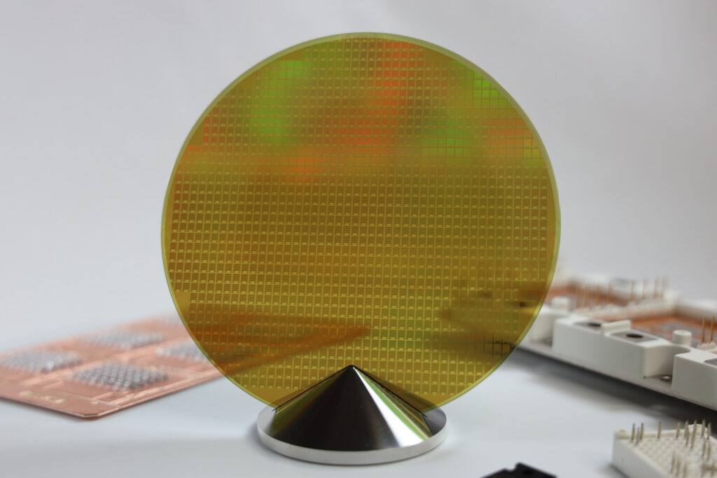
(Courtesy of Infineon)
SiC
SiC MOSFETs are built from numerous transistor cells arrayed side by side. To reduce overall device resistivity, the resistance of each cell must be reduced.
This is driving a move from today’s planar architecture, where the p-n-p junction of the MOSFET is lateral on the SiC wafer, to a vertical trench design where the n, p and n layers are stacked vertically.
This allows a denser array of cells but has created problems with insulation around the gate breaking down at high voltages. To tackle this, one company, Mitsubishi, has developed an electric field-limiting structure based on advanced simulations carried out during the design stage.
Reducing the electric field applied to the gate insulating film to that of a conventional planar-type level enables the film to achieve greater reliability at high voltage. This reduces the on-resistance by half, reducing heat generation and allowing the use of a smaller cooling device for energy savings and miniaturisation.
The electric field-limiting structure ensures device reliability by controlling current flowing through the semiconductor layer between the drain and source electrodes by applying a voltage to the gate electrode. To achieve control using a small voltage, a thin gate-insulating film is required.
If high voltage is applied in a trench-type power semiconductor device, a strong electric field can be concentrated in the gate and easily break the insulating film. To correct this, Mitsubishi has developed the electric field-limiting structure that protects the gate insulating film by implanting aluminium and nitrogen to change the electrical properties of the semiconductor layer, taking advantage of the trench structure.
First, aluminium is implanted vertically and a film is laid down on the bottom of the trench to provide more isolation. The electric field applied to the film is reduced to the level of a conventional planar power semiconductor device, improving reliability while maintaining the breakdown voltage of over 1500 V. The source electrode is formed by using a newly developed technique to implant aluminium in a particular pattern to enable high-speed switching and reduced switching loss.
Locally formed high-impurity doped layers achieve the low on-resistance, as the trench SiC MOSFET has transistor cells that are smaller than those of planar types. This allows more cells on a single chip.
To achieve this, Mitsubishi developed a new method for implanting nitrogen to form a local layer of SiC with a high concentration of nitrogen, which allows electricity to be conducted easily in the current path. As a result, even when cells are arrayed densely, resistivity can be reduced by about 25% compared to the case of no high-concentration layer.
The new manufacturing method also allows intervals of the side grounding to be optimised. The result is a specific on-resistance of 1.84 mΩ/cm2 at room temperature – about half that of planar designs – while maintaining the 1500 V breakdown voltage.
Infineon also uses a trench design for its 1200V MOSFETs. This gives 25% lower switching losses compared to Infineon’s first-generation planar devices and higher switching frequencies, which in turn leads to higher power density and smaller system sizes.
With a gate-source threshold voltage of over 4 V and a very low ratio between the feedback capacitance and input capacitance, the trench design provides reliable turn-off at a threshold voltage of 0 V without risking parasitic turn-on. This allows a simpler control system, significantly reducing system complexity and cost. The devices also have a lower on-resistance, which reduces conduction losses over the entire -55 to +175 ºC temperature range.
The package for the devices is also an important consideration, as this increases the overall resistance and can increase the losses. However, many of the packages are standardised by the international JEDEC organisation to allow devices form different manufacturers to be easily used in power electronics designs. This standardisation in size and footprint can limit the innovation to reduce the resistance though, so there is a focus on using different materials and structures inside the package to reduce the overall resistance without reducing overall reliability.
So-called Kelvin packages use a fourth lead alongside the emitter, base and collector of the transistor to spread out the current and reduce the overall resistance. There are also leadless packages that allow more space for a connection to the heat sink for cooling, allowing higher currents to be used.
The improved connection between the die and the cooling system reduces the junction temperature of this SiC MOSFET by 25% compared to the first generation. The MOSFET also features a creepage distance of 5.89 mm, meeting package-level requirements for 800 V systems. This leads to the only 9 mΩ variant currently available in a TO263-7 package.
Onsemi is also developing SiC MOSFETs using a trench structure rather than a planar one, with samples expected next year.
The company has an SiC wafer plant near Brno in Czechia (the Czech Republic) with device manufacturing at a lab in Korea. The move to a trench structure allows more devices to be built on a 150 mm wafer, driving down the cost of the devices. The company also has an engineering programme for 200 mm SiC wafer production. The trench design and the larger wafers will produce more devices on a wafer and thus bring down the cost.
The planar SiC devices are also used in half-bridge power integrated modules with a low on-resistance in a standard package for DC fast-charging designs.
The automotive-qualified 1200 V MOSFETs are tailored for high-power onboard chargers up to 22 kW and high voltage to low voltage DC-DC converters.
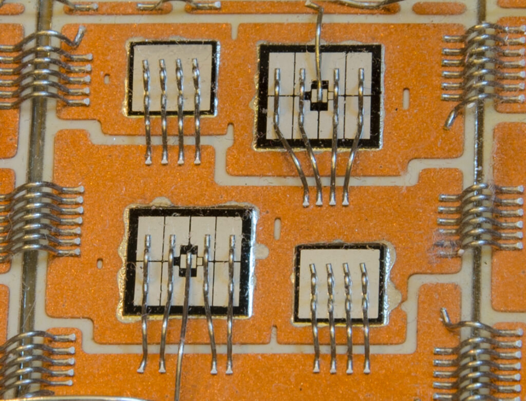
(Courtesy of GaN Systems)
GaN
GaN Systems has introduced its fourth generation of GaN architecture. The basic technology uses an ‘island’ structure that takes out the current from the planar HEMT transistor vertically, resulting in lower losses and frequencies as high as 20 MHz.
“We continue to make improvements in performance,” says Jim Witham, CEO of GaN Systems. “There are two knobs to turn – the fab process and design. We work on the process and the structure, which gives a 20% improvement in the figure of merit, which is the product of the charge carrier saturation velocity in the material and the electric breakdown field and used to determine the overall performance of a transistor, whether that is a HEMT GaN, IGBT or SiC MOSFET.
“The two major things we have done is electric field management and getting rid of white spaces – these are nonactive areas of the chip. Each customer application has a target on-resistance so we make a family of parts that then make the switching losses as low as possible.
“If the die is too small you can struggle to get the heat out, but a smaller die is less expensive so we tend to try to push the limits of the die and use the packaging to get as much heat out as possible. It’s still the case that packaging is important – for an extra cent of packaging you can save more than a cent in the die.
“Our fourth-generation technology is the same 100 V and 650 V products. We played a lot with 1200 V two level versus 650 V multi-level, and we found a lot of value in the multi-level designs.
“We like 650 V parts better in these applications. At 1200 V the dv/dt is much bigger than 650 V, and that reduction in the dv/dt gives you lower EMI and noise and lower losses. The EMI and the noise is more important for the filtering you need, and interference issues are becoming bigger,” he says.
This is even more important than the switching frequency increases.
“The DC-DC converter and OBC combo designs are the first place everyone goes, as you can push the frequencies up but the same thing is happening the traction inverter,” Witham says, “We have lots of activity in the inverters with higher switching frequencies.”
The OBC is typically at 10 to 200 kHz while the inverters are 10 to 20 kHz, driven mainly by the IGBT and SiC MOSFET requirements.
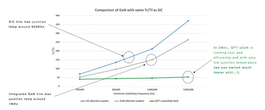
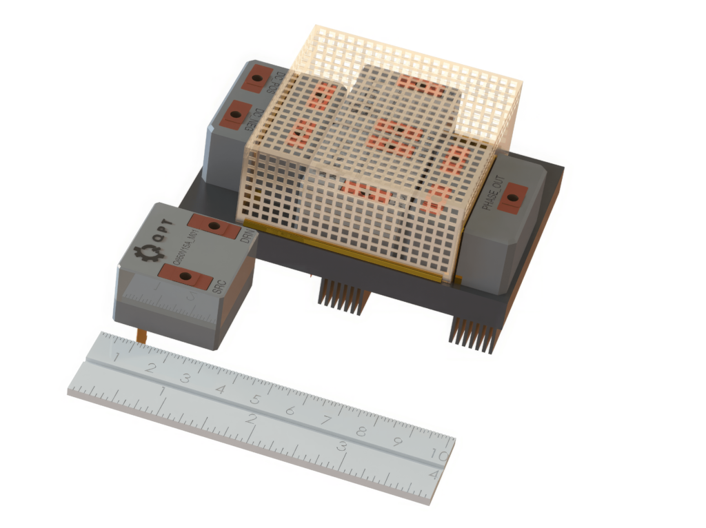
(Courtesy of QPT)
High-speed switching
Achieving higher switching speeds with GaN devices is a real challenge.
“We have worked out how to switch GaN transistors incredibly fast – it’s a microwave black art,” says Rob Gwynne, founder and CEO of QPT.
“We focused on GaN technology, as that’s the future, and quickly realised that people were having challenges,” he says. “The solution is a GaN transistor from GaN Systems with an isolated drive at high switching speeds. The design has a range of microwave signals, and getting power engineers to design these boards is impossible.
“For higher power, there is a more limited repertoire topologies for motors, and they were mostly using silicon. We have solved the problems with EMC and thermals that allow engineers to put together building blocks with GaN that will be more efficient and power-dense.
“GaN Systems produces the highest performing 650 V power GaN devices, which allows us to achieve the highest efficiency when combined with our technology. The better the efficiency of power usage, the greater the range of the EV.
“Our approach is to switch as fast as possible rather than slow the devices down. There is no parasitic diode so they switch like an RF device. The 3 x 2 mm die is switching 8 kW but there are no thermal conduits in the package to get the heat out, so the junction temperature goes up and it has to be de-rated,” Gwynne says.
As soon as you go up in frequency, above 100kHz, the thermal issues increase and the on-resistance goes up. The QPT design sees 20 W losses at 2 MHz compared to 100-130 W with other drivers and enables motors to be driven at up to 99.7% efficiency at peak load with hardly any decrease in efficiency at lower loads.
“This is a colossal problem, and we had to come up with nine patents to get the thermal energy out without creating the RF parasitics from all the metal that couples to the rest of the circuit,” Gwynne says. “So you need microwave expertise up to the GHz range because of the switching edge speeds, and if you don’t properly manage that with picohenry inductance-level interconnect and correct impedance matching it basically goes bang.
“This takes months of EM analysis of designs, which is outside the expertise of the power engineers. We do use exotic materials such as aluminium nitride [AlN] but the key is as you add that metal you need to do the GHz analysis to work out the coupling, so you need complex geometry that is developed iteratively. We have other patents on parts of the circuitry, the geometry of the packaging and how it relieves thermal stresses.”
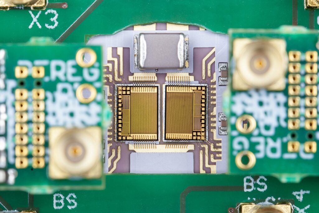
The first-generation modules measure 30 x 30 x 18 mm, and are a discrete solution as a proof of concept. A custom 650 V GaN transistor is being developed in parallel, but in the meantime the designs are using transistors from GaN Systems. QPT has developed reference designs and RF filters for the I/O and will be providing transistor modules and I/O modules. The modules will be an embedded die multi-level PCB with all the routing and drive circuitry and interconnect.
“We are switching in 1.5 and 2 ns on a 540 V bus, which is a high dV/dt, and there are no isolated gate drivers that can handle this, so we developed our own to switch kilowatts at this speed,” Gwynne says. “We are using silicon germanium (SiGe) for a high speed controller and a GaN pre-driver from EPC, and in the first ASIC we will have all that integrated into one SiGe part and integrated into layers of the PCB.”
The second-generation module being developed in parallel will be 5mm x 15mm x 15mm.
“The modules are built together on a plate, and there’s a Faraday cage on the top so there is nothing conducted and nothing radiated, so we can pre-qualify the system, making it easier to qualify,” Gwynne says. “The beautiful thing for us is that because we can operate in the 650 V regime we can do motors up to 500 kW for EVs.
“The Gen1 module is designed to work with pulse width modulation (see page 34) so it can be used with existing controller chips. These operate at up to 2 MHz with the TI C2000, but the drive technology works at up to 20-30 MHz so you can reduce the size of the converter tremendously,” he says.
(Courtesy of Fraunhofer)
Higher voltages
Toyoda Gosei and Powdec in Japan have developed a high-performance horizontal GaN power device for a 24 kW power converter. The Polarisation Super Junction GaN power transistor is a different structure to the HEMT devices and has a breakdown voltage of over 1500 V and a switching speed of 1 ms in an 800 V, 30 A module.
There are also opportunities to build GaN transistors on an SiC wafer for higher thermal performance. “GaN on SiC would be awesome but there is no multi-project wafer for that,” says Gwynne.
GaN reliability
The 11th report on GaN reliability from EPC in 2020 focused on reliability in automotive applications and found the transistors are more rugged than silicon devices. The Phase Eleven Reliability Report covered field experience of 123 billion device-hours over the previous 10 years for EPC’s enhanced GaN (eGaN) technology.
The field test strategy used in the report relied on tests forcing devices to fail under various conditions. This approach to GaN reliability creates an understanding of the margin between data sheet limits and products in application; more important, it identifies intrinsic failure mechanisms.
This knowledge of the intrinsic failure mechanisms is used to determine the root cause of failures. Knowledge of the behaviour of a device over time, temperature, electrical or mechanical stress can provide users with an accurate representation of the safe operating life of a product over a more general set of operating conditions.
“eGaN devices have been in volume production for over 10 years and have demonstrated very high reliability in both laboratory testing and high-volume customer applications,” says Dr Alex Lidow, CEO and co-founder of EPC.
“The release of EPC’s 11th reliability report represents the cumulative experience of using millions of devices over a 10-year period and five generations of technology. These tests have been undertaken to continue our understanding of the behaviour of GaN devices over a wide range of stress conditions.
“The results of our studies show that GaN is an extremely robust technology that continues to improve at a rapid pace. EPC is committed to subjecting GaN devices to rigid reliability standards and sharing the results with the power conversion industry,” he said.
The report shows that the key mechanisms impacting dynamic on-resistance have been identified and are used to create more robust designs. The result is that dynamic changes to on-resistance are not an issue for eGaN FETs.
Several eGaN products were tested over the data sheet safe operating area (SOA) and then taken to failure to probe the safety margins. The result showed that eGaN FETs will not fail when operated within the data sheet SOA.
eGaN devices are tested to destruction under short-circuit conditions to determine how long and what energy density they can withstand before catastrophic failure. The failures are thermally limited, and withstand time exceeds 10 µs at the recommended gate drive.
Conclusion
Different technologies are jostling for position in the development of power electronics for e-mobility applications. While silicon remains a stalwart for design engineers, with continuing development, the wide bandgap alternative of SiC and GaN are increasing the efficiency and performance of designs.
SiC is an easier alternative for silicon and provides higher efficiencies with a limited boost in the switching frequencies achievable. GaN offers the promise of far higher switching frequencies that could drive smaller sizes and even higher efficiencies, but the devices are extremely hard to design at this point. Emerging technology is allowing the full advantage of GaN in e-mobility, with the potential of switching beyond 2 MHz and as high as 20 MHz.
This will enable very different power electronics designs to boost the performance and efficiency of e-mobility platforms over the coming years.
Click here to read the latest issue of E-Mobility Engineering.
ONLINE PARTNERS

