


Power Semiconductors
(Courtesy of Fraunhofer IAF)
Band members
Nick Flaherty reports on how new semiconductor technologies with wider bandgaps will improve the efficiency of electric powertrains.
Most power systems for electromobility use semiconductor devices built using a silicon process, but new technologies are maturing that provide higher efficiency and so dissipate less heat, making those systems smaller or more powerful for the same size.
Metal oxide semiconductor field-effect transistors (MOSFETs) are used largely in charging systems, and are built using the same complementary metal-oxide semiconductor (CMOS) process used for most electronic chips. By contrast, the more powerful insulated gate bipolar transistors (IGBTs) are built using older chip-making processes but can handle higher voltages, so they are used more in traction motor drives and the inverters that convert energy from batteries.
IGBTs combine the simple gate-drive characteristics of MOSFETs with the high-current and low saturation voltage capability of bipolar transistors. They combine an isolated-gate FET for the control input and a bipolar power transistor as a switch in a single device.
One advantage with that is that multiple devices can be used in parallel to provide very high current-handling capabilities, of the order of hundreds of amperes, with blocking voltages of 6500 V, controlling loads of hundreds of kilowatts.
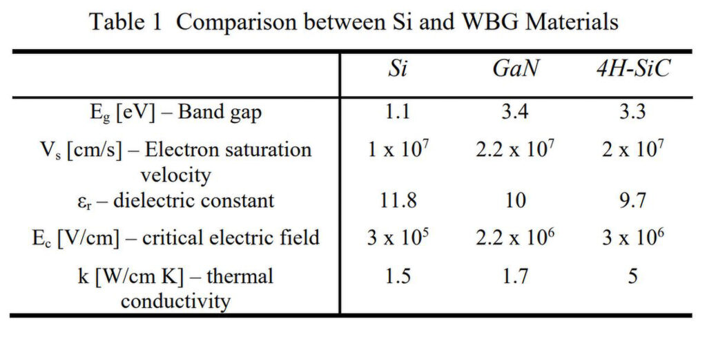
Both MOSFETs and IGBTs, with a bandgap of 1.1 eV, are used in half-and full-bridge converter topologies at frequencies of up to 50 kHz and efficiencies of around 85%. These are often combined with the gate drivers (built using a standard CMOS process) in modules where other factors such as the capacitance in the packaging can be optimised.
However, both technologies struggle with the megahertz-level operation and voltages of 600-1800 V that allow higher efficiency. The higher frequency operation is enabled by a wider bandgap, from materials such as silicon carbide (SiC) and gallium nitride (GaN).
Replacing MOSFETs and IGBTs with devices using wide-bandgap materials can increase the typical DC-DC converter efficiency from about 85% to nearer 95%, or boost typical DC-AC inverter efficiency from 96% to 99%.
For hybrid and electric vehicles, this higher efficiency allows automotive designers a set of architectural tradeoffs, from smaller and lighter battery packs to more efficient motors for longer ranges from existing packs. However, these devices have needed new packaging, which also leads to more long-term testing required for automotive qualification. They also often need new drivers (built from standard CMOS silicon), so the power subsystem has to be redesigned.
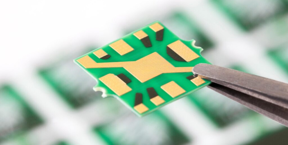
Silicon carbide
(Courtesy of UnitedSiC)
With a bandgap of 3 eV, SiC has a far higher critical electric field, better thermal conductivity and dielectric constant than silicon alone. It can therefore provide low on-resistance, low leakage current (even at higher temperatures) and better overall performance in high-temperature environments, making it the first wide bandgap material to make its way into cars and trucks.
Diodes and MOSFETs built using an SiC process have been qualified to the AEC-Q101 standard for use in automotive designs. A 1200 V planar Schottky diode built-in SiC, for example, has a total capacitive charge (Qc) that is small (65 nC), reducing switching losses and enabling faster operation. That has led to charger designs that are a tenth of the size and weight of those based on silicon devices, and with an efficiency of 97%.
These have been adopted in car designs since 2016. “Major car makers and automotive Tier 1 suppliers are now committing to silicon carbide technology for future product development because of its higher aggregate efficiency compared to standard silicon in a wide range of operating scenarios,” says Mario Aleo, group vice-president of STMicroelectronics and general manager of its Power Transistor division. ST launched its first 1200 V SiC MOSFET in 2014 with a 200 C rating that allows smaller charger designs.
One advantage with SiC is that the switching time is constant and does not vary with temperature. This allows less of a design margin for varying temperatures and makes the devices suitable for the inverters in electric vehicles. These use TO-220 packaging, but lower-voltage 650 V SiC diodes are using the smaller TO-263AB packaging (also known as SOT-23) to reduce the size of the power systems.
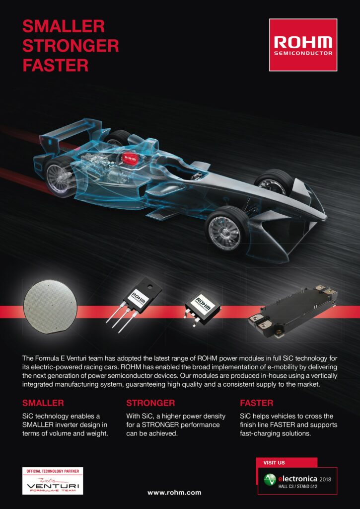
The Venturi Buckeye Bullet 3 electric vehicle holds the speed record for an electric car – 549 kph (341 mph) – using modules based on SiC MOSFETs from Rohm Semiconductor. The modules allowed the use of inverters that are a third of the size and weight of the previous generation developed by Rohm.
Pure SiC MOSFETs require new drivers, but new modules designed by UnitedSiC have allowed SiC devices to be used as drop-in replacements for IGBTs.
They combine a ‘normally on’ SiC JFET (junction gate field-effect transistor), rather than a MOSFET, that is packaged with a custom low-voltage silicon MOSFET in an ‘always off’ device. The retained charge (Qrr) of the combined devices is about a third of that for a silicon MOSFET, allowing faster operation and higher efficiency at 650 V but still using the existing gate driver chip.
This opens up new packaging options as the silicon MOSFET can be soldered onto the JFET, removing the need for the freewheeling diode usually required in a module. These are now being demonstrated to electric car makers.
UnitedSiC’s UJ3C series of modules use standard TO-220, TO-247 and D2PAK-3L packages, and operate with a standard silicon MOSFET gate drive, eliminating the need to redesign drive circuits while supporting more efficient switching topologies such as zero-voltage switching with switching frequencies of up to 500 kHz. This allows designers to reduce the size and cost of other system components, including bulky inductors, capacitors and thermal management parts.
For new designs the use of these SiC devices opens up new power conversion topologies, the most popular being totem-pole power factor correction (PFC). This is a design for the front end of a power system that can provide efficiencies as high as 99.2%.
Using silicon MOSFETs would require 14 separate devices and a highly complex controller. Using an SiC or GaN wide bandgap device, however, they can be implemented using only four transistors and much simpler control.
Tesla is the first high-class car maker to integrate a full SiC power module, in its Model 3. SiC MOSFETs from STMicroelectronics are used in 24 power modules assembled on a pin-fin heat sink.
Each module contains two SiC MOSFETs with a new die-attach approach to reduce the parasitic capacitances, connecting directly to the terminals of the module using copper clips and thermally dissipated by copper baseplates.
New process technologies are boosting the performance of SiC devices. For example, a developer of SiC epitaxial materials has moved into producing devices with a range of diodes rated to 1200 V, 1700 V and even 10 kV. MOSFET switches are also under development.
“We have developed a materials technology that makes it possible to handle very high power with minimal losses, while maintaining the reliability of silicon,” says Adolf Schöner, CTO of Ascatron. “We call it 3DSiC and it is based on our SiC epitaxy material. The technology has the potential to reduce losses by up to 30% compared to conventional solutions.”
Each device is divided in a high-voltage module, related to the desired voltage class and a low-voltage part for each type of component. Combining different modules gives a range of products.
Coming later than SiC, GaN has been only slowly adopted, owing to cost, yield and reliability concerns, according to Anup Bhalla, vice-president, engineering, at UnitedSiC. “GaN is certainly theoretically capable of faster switching than SiC or Si, with its much higher electron mobility, but with a thermal conductivity lower than SiC by a factor of three, its power density potential is limited,” he says.
“At the moment, SiC devices are common at around 650 V to 1.2 kV ratings and higher, while GaN is limited to around 650 V, where it struggles to compete with the lower cost and proven robustness of the more mature SiC offering at the same voltage. However, SiC devices also address the electromobility market, especially in applications for bidirectional DC-DC converters and totem-pole PFC.”
GaN suppliers are tackling the reliability concerns though, with detailed test results and by improving the technology.
Gallium nitride
GaN devices have a wider bandgap of 3.4 eV, and a higher electron mobility than SiC, which can provide an even higher conversion efficiency of 97%. This higher bandgap has been used for many years in the wireless market, but new versions of the technology are being adopted in power designs.
Lateral GaN transistors are built with horizontal rather than vertical junctions, and have improved switching characteristics over vertical silicon transistors, but are comparable to silicon super-junction MOSFETs in terms of the conduction losses per unit semiconductor area. However, new device structures using the enhancement mode of GaN have allowed higher performance by eliminating the bulk capacitance.
650 V GaN transistors built on a silicon substrate allow for higher currents and voltage breakdowns than SiC or silicon, leading to switching frequencies of more than 100 MHz. These new transistor layouts boost the high-current die performance and the yield, which are key factors for electromobility designs, says Jim Witham, CEO of GaN Systems.
Traction inverters are sized for current, and that application is dominated by conduction losses, but there’s little difference between GaN, silicon and SiC. However, the load profile shows that more time is spent at low load, such as around an urban environment. This low-load operation is where GaN dominates with lower switching losses, so designs are split between high voltage using silicon IGBTs and medium- and low-voltage systems that are moving to GaN.
“The sweet spot is 100 to 1200 V, and from a few amps to hundreds of amps,” Witham says. “Every company in the automotive space has GaN designs in the works right now – the weight and volume are really critical, to get longer range or use fewer batteries, and GaN is more efficient than silicon or silicon carbide.
As mentioned, one of the key areas of concern with GaN transistors has been reliability and the ability of the devices to meet the AEC automotive reliability standard.
“We have detailed test programmes with all the automotive manufacturers for AEC automotive qualification, they have all the test results we have performed,” Witham says. The devices have already been designed into an onboard charger for car maker BMW, which is a third of the size and weight of a traditional silicon one, and another for subsystem supplier Hella that is one-fifth the size of previous versions Hella has developed.
“The three most common applications are onboard chargers, DC-DC converters and traction inverters, and that’s where most people are using the GaN devices,” Witham says. “If you can’t charge your car it won’t run, so charging is a critical function. I can’t think of any case where the engineering team doing the traction and converters don’t also do the charger.”
GaN technology is evolving, with the third-generation 650 V devices providing greater immunity to gate noise (up from 2.1 to 4 V), giving more headroom in circuit design applications.
Packaging
With higher frequency and higher power operation, packaging is also an important factor.
New proprietary packaging techniques for the GaN devices can improve system performance, but proprietary packages can also restrict the availability of devices for high-volume production. To address this, GaN Systems for example has signed a deal with Japanese supplier Rohm to use GaN Systems’ packaging technology to provide a second source for car makers.
Similarly, the latest 50 mΩ and 35 mΩ GaN FETs from Transphorm are packaged in standard TO-247 packages, making dual sourcing easier.
New packaging technologies can also provide higher levels of integration. Researchers at Fraunhofer IAF in Germany, for example, have developed a fully integrated monolithic converter using high-voltage AlGaN/ GaN-on-Si technology.
The integrated converter circuit is designed for a maximum voltage of ±400 V and a current of 5 A, and is built from four transistors and six diodes.
Packaging the die was a key consideration for the converter. If lateral components are used, the source, drain and gate pads are on one side and the back of the die is used for heat dissipation.
The conventional approach of using wires to connect the die to the circuit board restricts the overall performance of the design, so instead an embedded substrate technology from AT&S was used with the power devices embedded into the PCB material and connected from both sides.
The chips are connected directly via low-impedance copper-plated connections, or microvias, that significantly lower the inductance compared with wire bond technology. The rear of the die is also connected by means of copper-plated microvias to improve heat dissipation.
“We see this mounting technology as opening up entirely new possibilities – particularly for more complex monolithic integrated GaN power circuits, as used on our multi-level converter chip,” says Richard Reiner, a researcher at Fraunhofer IAF. “With a conventional design, we were hardly able to use and/ or evaluate the power chip.”
Dietmar Drofenik, CEO of the advanced packaging business unit at AT&S, says, “For wide bandgap semiconductor materials such as GaN in particular, the embedding technology makes miniaturised power packages possible for higher efficiencies, enhanced thermal performance and higher power densities.”
Vertical devices
(Courtesy of Imec)
For applications beyond 650 V, such as electric cars and renewable energy, it has become difficult to further increase the buffer thickness on 200 mm wafers to the levels required for higher breakdown voltages and low leakage levels, because of the mismatch in the coefficients of thermal expansion (CTE) between the GaN/AlGaN epitaxial layers and the silicon substrate.
Thicker silicon substrates could be used to keep wafer warp and bow under control for 900 and 1200 V applications, but that has caused compatibility issues in wafer handling in some processing tools, meaning some of those tools are unable to handle the wafers.
There is also a move from lateral GaN devices to vertical structures that will be much cheaper to make on 200 mm silicon wafers. Belgian research house Imec, for example, has worked with Qromis to produce 650 V enhancement mode GaN devices on 200 mm engineered CTE-matched substrates, processed in Imec’s silicon pilot line.
Imec used a CTE-matched core with a thermal expansion that very closely matches that of the GaN/ AlGaN epitaxial layers to build 900 and 1200 V devices on standard thickness 200 mm wafers. This also opens up the possibility of building vertical GaN power switches and rectifiers suitable for high-voltage and high-current applications currently dominated by silicon IGBTs, SiC power FETs and diodes.
Magnetics
While the higher switching speed of wide bandgap devices can be up to 100 MHz, with low losses at high power and temperatures, the magnetics are struggling to keep up, especially with low losses. Practical low-loss designs have been achieved with SiC, for example at more than 100 kW at relatively low frequencies that keep the cost of the ferrite material used in the inductors at a reasonable level and still provide low core losses.
The currents that go along with these high-power designs are leading to more planar magnetics with, typically, stamped copper windings for the inductor and with the assembly actively cooled using water plates or fans.
Planar magnetics at high power and frequency also allow close control of parasitic losses such as leakage inductance. This can be vital in conversion topologies that use leakage inductance as part of a resonant network to obtain low-loss switching.
Drivers
“These days the GaN FETs are all a bit different, so you need different drivers,” says Steve Tom, GaN Systems’ product line manager at Texas Instruments (TI). “It will be interesting to see if these drivers converge, and to do that you will have to give up a bit of performance.”
The latest drivers from TI now support switching frequencies up to 50 MHz, up from just 1 MHz previously. “We had customers who wanted 6 MHz, and with a 50 MHz part they can go as fast as they want,” he says. “It will be interesting to see what they do with that additional performance.”
“A lot of times at high speeds you can drive MOSFETs, so our 50 MHz device can drive silicon or GaN,” he adds. “In 600 V we are integrating the driver and the FET together so they are optimised together – co-packaging – where our present thought is there is a lot of benefit for the silicon driver and integrating the current limit protection for fast short-circuit protection with a good signal-to-noise ratio.
“You can do a lot of integration in GaN but if we are going to put everything into a package then the end-user doesn’t worry too much about what’s in it.”
There are now moves to build the driver in GaN rather than silicon so that it can be integrated in a monolithic chip. Efficient Power Conversion, for example, has integrated the driver with a 200 V, 40 mΩ enhancement-mode monolithic GaN power transistor for lower power charger designs, and has developed a device with two 150 V, 70 mΩ GaN FETs plus gate drivers.
Both can operate at up to 7 MHz and are available in a 2.9 x 1.1 mm BGA surface-mount passivated die, highlighting the advantage of integrating the driver into the chip.
Other uses
Other wide bandgap materials can be used in a number of electromobility applications. Aluminium nitride (AlN) for example has a bandgap of more than 6 eV, opening up applications in LEDs by using AlN alloys alongside GaN LED devices. These are being developed for headlights and interior lighting applications in electric vehicles.
Another wide bandgap material, boron nitride (BN), is suitable as a substrate for high-power systems. Plastics filled with BN have less thermal expansion as well as higher thermal conductivity and electrical resistivity.
Silicon carbide devices have been tried and tested in electromobility designs for the past decade, providing reliability data and the ability to drop modules into existing systems using silicon IGBTs, and so are the dominant wide bandgap technology at the moment, particularly for traction designs. Designers are now adopting GaN technology more widely though, starting with the onboard chargers and moving into other parts of a vehicle.
ONLINE PARTNERS
